Advertisement
)

AT A GLANCE
- Concept: ASML: The Dutch engineering conglomerate holding an absolute global monopoly on extreme ultraviolet scanners.
- Concept: EUV Light: An artificial 13.5-nanometer wavelength required to print atomic-scale transistors on silicon.
- Concept: Laser-Produced Plasma: Vaporizing liquid tin droplets with industrial lasers to generate the required ultraviolet light.
- Concept: Reflective Optics: Using specialized mirrors instead of glass lenses because EUV light absorbs into physical matter.
IN SIMPLE WORDS
Imagine trying to paint a highly detailed portrait on a grain of rice. If you use a thick paintbrush, the lines will blur together into a meaningless blob. To paint smaller details, you need a single hair.
For decades, the computer industry used deep ultraviolet light to print computer chips. As chips became more advanced, the “brush” became too thick. The circuits blurred.
A Dutch company named ASML spent three decades inventing a smaller brush. They created Extreme Ultraviolet (EUV) lithography, a machine that generates light with a wavelength so short it can print features just a few atoms wide.
Because building this machine is so mathematically and physically difficult, ASML is the only company on Earth that successfully makes them. Without this single company, the global production of modern smartphones, advanced artificial intelligence, and military hardware physically stops.
HOW IT WORKS
Printing a modern microchip requires moving beyond the natural spectrum of light. The features on a sub-3nm transistor are so small that regular light waves simply wash over them without transferring the pattern. Engineers must synthesize Extreme Ultraviolet (EUV) light at exactly 13.5 nanometers.
Creating this specific wavelength requires extreme thermodynamic violence. Inside the ASML scanner, a mechanical generator fires 50,000 microscopic droplets of molten tin into a vacuum chamber every second.
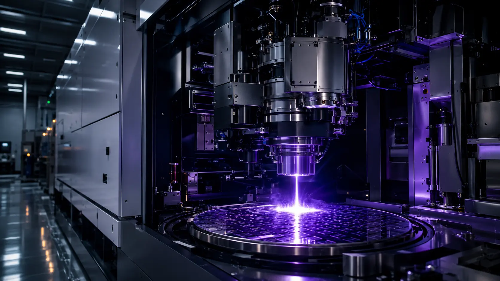
A high-power carbon dioxide laser fires twice at each falling droplet. The first pulse flattens the tin into a disc, and the second massive pulse vaporizes it into a highly charged plasma. As this plasma cools, it emits the required 13.5nm light.
Once generated, this light faces an immediate physical problem. EUV light is absorbed by almost all matter, including regular air and standard glass lenses. You cannot focus it using traditional optics.
Instead, the machine operates entirely in a vacuum and uses Bragg reflectors—perfectly smooth mirrors built from alternating layers of silicon and molybdenum. These mirrors bounce the light back and forth, refining the beam before reflecting it off a master stencil called a reticle.
The light carries the stencil’s pattern down onto the silicon wafer, exposing a photo-sensitive chemical layer to print the circuitry.
REAL WORLD EXAMPLE
When Apple designs the latest processor for the iPhone, that chip contains roughly twenty billion individual transistors. Apple does not build this chip; it sends the design to TSMC, a massive semiconductor foundry in Taiwan.
TSMC can only fulfill Apple’s order because it operates dozens of ASML EUV scanners. To print the absolute smallest features of the M-series or A-series chips, the TSMC factory floor must align the wafer inside the scanner with nanometer precision.
If TSMC’s ASML machines experience a power failure or a laser misalignment, the entire Apple supply chain stalls. The physical delivery of consumer hardware worldwide is strictly throttled by the uptime of these specific Dutch machines.
WHY IT MATTERS NOW
The current artificial intelligence boom relies entirely on brute computational force. Training massive models like GPT-4 requires tens of thousands of Nvidia H100 graphics processing units (GPUs).
These specific chips pack 80 billion transistors into a single piece of silicon. They demand extreme power efficiency and processing density that only EUV lithography can physically produce. The global AI arms race is functionally a race to secure EUV production capacity.
This physical reality turns ASML into a geopolitical chokepoint. The United States recognizes that whoever controls the hardware controls the future of artificial intelligence, cryptography, and automated warfare.
Consequently, the US government actively enforces strict export controls, legally barring ASML from selling its most advanced EUV scanners to Chinese foundries. This singular policy creates a structural ceiling on rival semiconductor programs, forcing them to rely on older, less efficient multi-patterning techniques.
COMMON MISCONCEPTIONS
Many assume ASML builds the entire machine in-house. In reality, ASML acts as an advanced systems integrator. The critical mirrors come exclusively from Zeiss in Germany, and the high-power drive lasers come from TRUMPF.
Observers often think more laser power automatically equals faster chip production. They miss that higher power drastically increases thermal stress, physically warping the protective pellicle membrane that shields the stencil from falling dust.
People frequently confuse chip design with chip manufacturing. Companies like Nvidia and AMD do not actually possess the physical ability to make their own products. They are entirely dependent on foundries that buy ASML scanners.
WHAT MOST PEOPLE MISS
Economic commentators view the 350-million-dollar price tag of a High-NA EUV machine as the primary barrier to entry. They completely overlook the operational physics required just to turn the machine on.
A single EUV scanner consumes over a megawatt of continuous electricity. The laser-plasma process is incredibly inefficient, converting only a tiny fraction of the input power into actual 13.5nm light. The rest turns into massive waste heat.
Building an EUV factory requires constructing dedicated power plants, massive water-cooling infrastructure, and nitrogen gas pipelines just to support the scanners. The true moat is not buying the machine; it is affording the immense energy and chemical logistics required to feed it daily.
THE ECONOMIC AND STRATEGIC IMPACT
ASML holds absolute pricing power over the global semiconductor logic market. Foundries like TSMC, Intel, and Samsung have no alternative suppliers. They must pay whatever ASML demands to stay relevant in the sub-3nm chip race.
This monopoly shifts the financial dynamics of the entire technology sector. As the machines become more expensive, the capital expenditure required to build a leading-edge fab exceeds twenty billion dollars. This cost barrier bankrupts smaller foundries, forcing rapid consolidation in the manufacturing sector.
Strategically, the US, Europe, and Japan benefit immensely from keeping this supply chain anchored in allied territories. The nation that hosts the physical EUV machines dictates which companies, and by extension which militaries, receive the most advanced computing hardware.
THE TRAJECTORY
Next 12–36 Months: Foundries will transition to High-Numerical Aperture (High-NA) EUV. These massive new machines feature larger, reshaped mirrors that capture light at wider angles, allowing engineers to print 2-nanometer features without running the silicon through the scanner twice.
Next Five Years: The materials science of the pellicle membrane will become the primary bottleneck. As scanner light sources push toward 500 watts, traditional silicon-based dust covers will melt. Chemical suppliers will commercialize carbon nanotube pellicles to survive the extreme thermal load.
Next Ten Years: The industry will hit the absolute geometric limit of High-NA optics. Foundries will begin exploring Hyper-NA systems or entirely new light generation methods, such as free-electron lasers housed in stadium-sized particle accelerators, to bypass the inefficiency of tin plasma.
What Could Go Wrong: Zeiss mirror supply constraints. The mirrors inside a High-NA scanner are so perfectly polished that if they were the size of the Earth, the tallest mountain would be a millimeter high. A disruption at the single German facility capable of this polishing halts global EUV production entirely.
Most Likely Outcome: ASML will maintain its monopoly for the foreseeable future. The sheer complexity of synchronizing lasers, plasma, vacuum chambers, and atomic-scale mirrors requires decades of proprietary trial and error that rival nations cannot simply reverse-engineer.
KEY TERMS
- Extreme Ultraviolet (EUV): Light with a wavelength of 13.5 nanometers used exclusively to print microscopic transistors on advanced silicon wafers.
- Laser-Produced Plasma (LPP): The physical process of vaporizing liquid metal with a high-power laser to generate a specific wavelength of light.
- High-Numerical Aperture (High-NA): An advanced optical system that uses larger mirrors to capture light at wider angles, increasing the printing resolution of the scanner.
- Reticle: The master stencil or mask that holds the physical blueprint of the microchip pattern being printed.
- Bragg Reflector: A highly specialized mirror made of alternating atomic layers designed to reflect specific wavelengths of light that normal glass would absorb.
- Pellicle: An ultra-thin protective membrane stretched across the reticle to prevent microscopic dust from ruining the chip pattern.
BEGINNER FAQ
What does ASML stand for? It originally stood for Advanced Semiconductor Materials Lithography. Today, the company simply goes by the acronym ASML and operates out of Veldhoven in the Netherlands.
Why can’t other companies build EUV machines? The machine requires integrating technologies from hundreds of highly specialized global suppliers. Replicating the decades of proprietary software, optical physics, and material science required to make these parts work together is practically impossible for a new competitor.
How big is an EUV scanner? A standard EUV scanner is roughly the size of a city bus and weighs over 180 tons. Moving a single machine requires multiple Boeing 747 cargo flights and dozens of shipping containers.
Why does EUV light have to operate in a vacuum? EUV light at 13.5 nanometers is highly energetic and absorbs into nearly everything it touches. If there were normal air inside the machine, the oxygen and nitrogen molecules would absorb the light before it ever reached the silicon wafer.
What happens to the tin after it gets zapped by the laser? The vaporized tin turns into microscopic debris and plasma exhaust. The machine constantly injects high-speed hydrogen gas into the chamber to sweep this debris away before it can coat and ruin the expensive mirrors.
How many chips can one machine print? A modern EUV scanner can process over 160 silicon wafers per hour. Since each wafer holds hundreds of individual chips, a single machine prints thousands of advanced processors daily.
Why doesn’t ASML make the chips themselves? ASML specializes entirely in lithography equipment engineering. Building a factory to actually manufacture the chips requires a completely different set of skills involving chemical etching, material doping, and advanced packaging that companies like TSMC specialize in.
Can China build its own EUV machine? Currently, no. While Chinese firms are heavily investing in domestic lithography research, they are blocked from buying the critical German optics and American lasers required to stabilize the EUV plasma process.
SOURCES
- ASML — The Physics of Extreme Ultraviolet Lithography and High-NA Systems
- SPIE (International Society for Optics and Photonics) — Laser-Produced Plasma Light Sources for Sub-3nm Scaling
- Massachusetts Institute of Technology (MIT) — The Geopolitics of Semiconductor Supply Chains and Export Controls
- Center for Strategic and International Studies (CSIS) — Chokepoints in the Global Semiconductor Industry