Advertisement
)
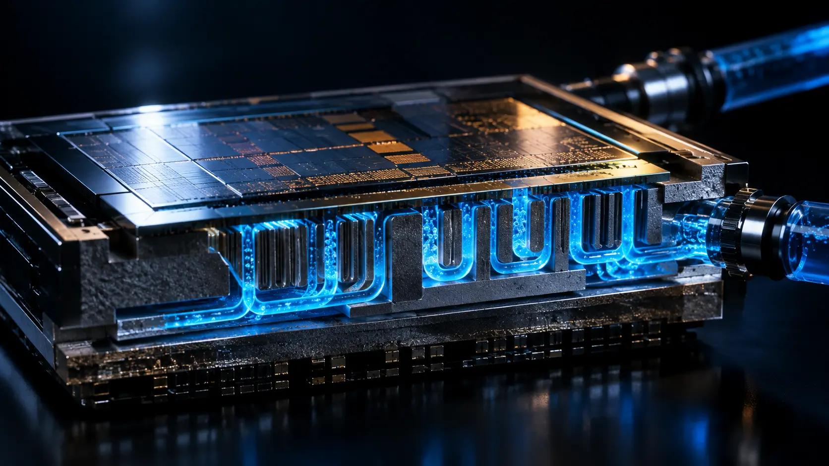

The global artificial intelligence race is currently colliding with a brutal, unavoidable wall of thermodynamics. Next-generation AI accelerators are crossing a heat flux threshold of 500 watts per square centimeter—a thermal density approaching that of a nuclear reactor fuel rod. Traditional cooling methods rely on slapping a cold metal plate onto the top of the chip, but the microscopic layers of glue and copper between the coolant and the transistors act as thermal insulators. The heat becomes trapped, the silicon chokes, and the multi-million-dollar AI training run halts.
Why should you care right now? Because semiconductor engineers are bypassing the surface entirely and drilling microscopic plumbing directly through the middle of the silicon die. By pumping liquid coolant inside the chip itself, literally micrometers away from the active transistors, the industry is breaking the ultimate thermal resistance barrier. This sub-micron microfluidic cooling fundamentally rewrites the geometry of high-performance computing, rescuing the next generation of AI data centers from a physical, silicon-melting bottleneck.
What is Sub-Micron Microfluidic Silicon Cooling?
Sub-Micron Microfluidic Silicon Cooling is an advanced direct-die immersion and thermal management technology that etches microscopic channels directly into the backside of a semiconductor die. By pumping liquid coolant through these internal pathways, it removes heat directly from the transistors, bypassing traditional thermal resistance barriers to cool ultra-high-density AI accelerators.
At a Glance
- The Thermodynamic Problem: AI chips generate immense heat. Traditional cold plates require heat to travel through silicon, thermal paste, and copper lids, acting like an insulating blanket.
- The Microfluidic Solution: Carve microscopic rivers directly into the back of the silicon chip itself, removing the insulating layers entirely.
- The Mechanism: Dielectric fluid is pumped through these micro-trenches. As the transistors heat up, the fluid absorbs the heat instantly (sometimes boiling into a vapor) and carries it out of the chip.
- The Strategic Value: It enables a 10x increase in compute density. It unlocks true 3D-stacked chips (logic-on-logic), allowing data centers to build hyper-dense supercomputers without melting the hardware.
In Simple Words
Imagine a high-performance car engine running so hot it threatens to melt itself.
Traditional Cold Plate Cooling is like strapping massive ice packs to the hood of the car. The cold has to travel through the metal hood and the air gap before it ever reaches the engine block. A lot of cooling power is wasted just penetrating the outer layers.
Microfluidic Silicon Cooling is how a real car engine actually works. You drill channels directly through the solid metal of the engine block and pump cold water right next to the cylinders where the explosions happen. Semiconductor engineers are doing exactly this—treating the microscopic silicon chip like an engine block, etching tiny pipes through the silicon so the cold liquid flows directly behind the electrical “cylinders” (the transistors).
Why This Matters
For Semiconductor Engineers, Data Center VCs, and Thermal Architects, microfluidic cooling destroys the TIM Wall.
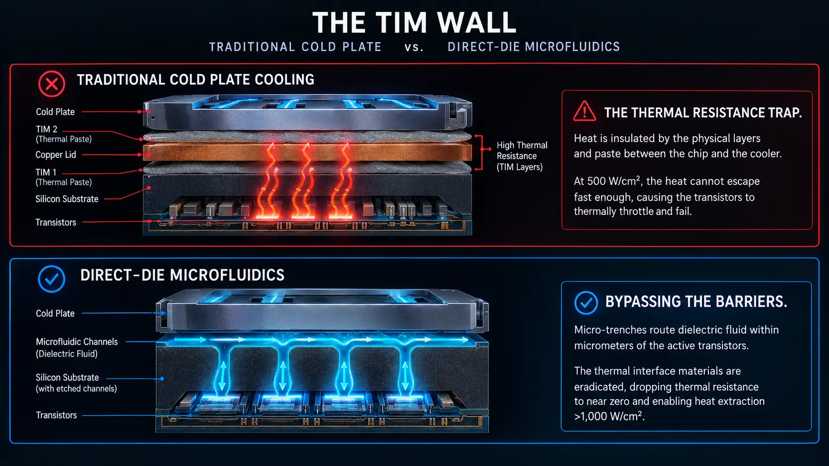
In thermal architecture, a Thermal Interface Material (TIM)—the grey thermal paste applied between a chip and a cooler—is a necessary evil. It fills microscopic air gaps, but its thermal conductivity is terrible compared to solid silicon or copper. In modern 1,000-watt GPUs, the TIM accounts for over 50% of the total thermal resistance in the system.
By running fluid directly inside the silicon, the TIM is entirely eliminated. The thermal resistance drops to near zero. For Data Center VCs, this is a paradigm shift: the limiting factor for AI cluster density is no longer the cooling infrastructure of the building, but the fluid dynamics inside the chip itself.
Micro-Insight: We are migrating from facility-level cooling (HVACs) to rack-level cooling (CDUs), and now, to die-level cooling. The HVAC system is moving inside the semiconductor.
Unlocking 3D ICs with Microfluidic Silicon Cooling
We are witnessing the Unlocking of True 3D Integrated Circuits (3D ICs).
The semiconductor industry wants to stack processing chips directly on top of each other like pancakes (logic-on-logic) to increase speed and reduce latency. However, if you stack two hot AI chips together, the bottom chip acts like an oven, trapping heat and instantly destroying the stack. Microfluidic cooling is the missing puzzle piece for 3D IC thermal management. By running a microfluidic cooling layer between the stacked silicon dies, engineers can extract the heat horizontally, allowing limitless vertical scaling of computer chips.
How Sub-Micron Microfluidic Silicon Cooling Works
Etching a vascular system into the brain of a computer without causing a short circuit requires absolute mastery of material science. Here is the first-principles breakdown of the architecture.
1. The Fundamental Problem: The Thermal Stack
In a standard server, heat must travel a long, inefficient path: from the transistor → through the bulk silicon → through the first TIM layer → through the copper integrated heat spreader (IHS) → through the second TIM layer → and finally into the liquid cold plate. Each boundary creates friction. At 500 W/cm², this friction causes the transistor temperature to skyrocket past its 105°C failure point, triggering thermal throttling.
2. The Core Mechanism: Deep Reactive Ion Etching (DRIE)
Engineers take the bare silicon wafer and use Deep Reactive Ion Etching (DRIE)—a highly precise plasma etching technique developed for micro-electromechanical systems (MEMS). They carve microscopic trenches, usually 20 to 100 micrometers wide, directly into the inactive backside of the silicon die. A glass or silicon lid is then bonded over the trenches to seal them, creating closed microscopic pipes.
3. Technical Depth: Pumping the Dielectric Fluid
A non-conductive (dielectric) engineered fluid is pumped into the chip at high pressure. Because the fluid is dielectric, even if a microscopic leak occurs, it will not short-circuit the electrical transistors. The fluid flows through the micro-trenches, passing within tens of micrometers of the active transistor junctions, absorbing the heat almost instantaneously.
Plain-English Takeaway: The chip is essentially hollowed out from the back, capped with a glass lid, and turned into a microscopic, high-pressure radiator.
4. Technical Depth: Two-Phase Boiling (Latent Heat)
There are two ways to use the fluid:
- Single-Phase: The fluid stays a liquid, simply warming up as it passes through the chip.
- Two-Phase: The pressure and chemistry of the fluid are tuned so that when it absorbs the transistor’s intense heat, it instantly boils into a vapor inside the micro-channel. Boiling requires massive amounts of energy (latent heat of vaporization). two-phase microfluidic cooling can absorb significantly more heat flux (often >1,000 W/cm²) than single-phase liquid, though managing the bubbles inside microscopic channels is incredibly complex.
5. Real-World Consequences: Pressure Drops and Pumping Power
The biggest physical constraint is fluid dynamics. Pushing liquid through a pipe that is thinner than a human hair requires extreme pressure. If the channels are too thin, the energy required to pump the fluid (pumping power) becomes so high that it negates the energy savings of the cooling system. Engineers must mathematically balance the surface area of the cooling trenches against the hydraulic resistance of the fluid flow.
Chip Cooling Architecture Simulator
Traditional Cold Plate vs. Sub-Micron Microfluidic Direct-Die Immersion
AI Chip Heat Flux
250 W/cm²
Cooling Architecture
Traditional Cold Plate
Direct-Die Microfluidic
Junction Temp (Tj)
68.5 °C
Thermal Resistance
0.18 K/W
System Status
NOMINAL
Die Cross-Section & Thermal Gradient Visualization
THERMAL EQUILIBRIUM
Transistor Temperature (°C) vs. Chip Heat Flux (W/cm²)
Real-World Applications
Sub-micron microfluidics is moving from DARPA research labs into the commercial roadmaps of global semiconductor foundries.
The DARPA ICECool Program: The Intrachip/Interchip Enhanced Cooling (ICECool) program was a foundational military research initiative that successfully demonstrated the viability of embedding microfluidic cooling directly into electronic substrates. It proved that defense radar systems and high-power radio frequency (RF) amplifiers could achieve massive performance boosts by replacing external heat sinks with internal, two-phase evaporative cooling channels, setting the stage for commercial data center adoption.
Imec's 3D-SOC Microfluidic Prototypes: Imec, the world-leading semiconductor research institute in Belgium, has actively prototyped 3D systems-on-chip (3D-SOCs) integrated with microfluidics. They successfully etched micro-impingement coolers into silicon using standard CMOS manufacturing techniques. By pumping fluid directly between vertically stacked silicon layers, they demonstrated the ability to dissipate over 600 W/cm² of heat, proving that 3D logic-on-logic stacking is thermally viable for future AI architectures.
TSMC direct-water cooling research: Taiwan Semiconductor Manufacturing Company (TSMC), the manufacturer of Nvidia's AI chips, has published extensive research on integrating micro-cooling systems. Their research explores etching silicon micro-channels directly onto the backside of the silicon interposer (the foundation that connects the GPU and the High-Bandwidth Memory). This brings the fluid as close as physically possible to the heat sources, signaling a clear roadmap for future 3nm and 2nm AI packaging.
Economic & Strategic Impact
The core strategic consequence of Direct-Die Microfluidics is Data Center Spatial Deflation.
Currently, data centers are sprawling outward. Because air cooling and cold plates are relatively inefficient, server racks can only host a limited number of AI GPUs before the rack overheats (often capping out around 40-100 kW per rack). To build a supercomputer, a cloud provider must lease a massive, warehouse-scale building simply to space the chips out.
Microfluidics allows for hyper-densification. If thermal limits are removed, engineers can pack hundreds of AI chips into a single, tightly compressed 3D blade. A supercomputer that previously required a 50,000-square-foot warehouse can theoretically be collapsed into a structure the size of a single refrigerator. This radically reduces data center real estate costs, shortens the electrical pathways (saving massive amounts of power), and fundamentally alters the economics of AI infrastructure construction.
Advantages of Direct-Die Immersion Cooling
- Destroys Thermal Resistance: Eradicates the need for Thermal Interface Materials (TIMs) and integrated heat spreaders (IHS), extracting heat directly from the silicon source.
- Enables 3D IC Stacking: Provides the only viable thermal management solution for vertically stacking hot, high-performance logic chips on top of one another.
- Extreme Heat Flux Capacity: Capable of dissipating well over 1,000 W/cm² using two-phase boiling, future-proofing cooling for the next decade of Moore's Law.
- Reduces Total Power Usage Effectiveness (PUE): Because heat extraction is so efficient, the cooling fluid can be supplied at higher temperatures (e.g., 40°C), reducing the reliance on massive, power-hungry facility chiller plants.
Engineering Limitations of Die-Level Microfluidics
- Extreme Pumping Pressure: Pushing liquid through 50-micrometer channels requires immense pressure. The hydraulic resistance requires powerful micro-pumps that are prone to mechanical failure.
- Channel Erosion and Clogging: Over a 5-to-10-year server lifespan, the high-pressure fluid can slowly erode the silicon channels. Even a microscopic particle of debris in the fluid loop can instantly clog a channel, causing catastrophic localized overheating (dry-out).
- Manufacturing Cost: Etching microscopic plumbing into every single silicon die requires additional, expensive lithography and etching steps at the foundry, significantly increasing the unit cost of the semiconductor.
Takeaway: The physics of microfluidics are flawless, but the mechanics are brutal. Ensuring that thousands of microscopic silicon pipes do not clog, leak, or erode over a 5-year data center lifespan is a monumental engineering challenge.
Common Misconceptions
Misconception: The computer chips have water flowing through the electricity.
Reality: The chips use engineered, highly dielectric (non-conductive) fluids. Even if the fluid comes into direct contact with the electrical transistors, it will not cause a short circuit.
Misconception: This replaces the need for data center cooling loops.
Reality: Microfluidics only moves the heat out of the chip. The hot fluid must still be pumped out of the server rack and routed to a massive facility-level heat exchanger (CDU) to dump the heat outside the building.
Misconception: Microchannels weaken the silicon structure, making it fragile.
Reality: While they remove bulk material, the channels are etched into the thick, inactive backside of the silicon substrate. When properly capped and bonded, the structural integrity of the die remains robust enough for standard server deployment.
What Most People Miss
The disruptive collision with Backside Power Delivery Networks (BSPDN).
To build faster chips, the semiconductor industry is moving power delivery to the back of the chip. In traditional chips, power and data both route through the top layer, causing traffic jams. Architectures like Intel's PowerVia route all the electrical power through the backside of the silicon, leaving the top entirely for data signaling.
This creates a massive geographical conflict. Microfluidic cooling also requires the backside of the silicon die to etch its plumbing. You cannot easily drill water pipes through the exact same microscopic real estate where you are laying the primary electrical power grid. Co-integrating Backside Power Delivery with Backside Microfluidics is the defining architectural war of the late 2020s.
Comparison Table
| Metric | Forced Air Cooling | Cold Plate (Direct-to-Chip) | Sub-Micron Microfluidics |
| Max Heat Flux Limit | ~100 W/cm² | ~300 - 500 W/cm² | > 1,000 W/cm² |
| Thermal Interface (TIM) Barrier | Severe | Moderate to Severe | None (Bypassed) |
| Pumping Power / Pressure Required | Low (Fans) | Moderate (Pumps) | Extremely High (Micro-pumps) |
| Enables True 3D Logic Stacking | No | No | Yes |
| Manufacturing Complexity | Standard | Standard | Extremely High (DRIE Etching required) |
Future Outlook
Next 12–24 Months
The era of 2.5D Interposer Microfluidics. Over the next two years, we will likely see the first commercial deployments not inside the main GPU die, but inside the silicon interposer—the foundational layer that connects the GPU to its memory. This is easier to manufacture and serves as the perfect testing ground to validate fluid flow, pressure drops, and pump reliability in a live data center environment without risking the main, expensive AI logic die.
Next 3–5 Years
The scaling of Two-Phase Co-Packaged Optics and Cooling. As data centers transition to co-packaged optics (replacing copper data cables with lasers directly on the chip), thermal tolerances will tighten. Lasers fail at much lower temperatures than silicon. Two-phase microfluidic cooling will be aggressively deployed to keep these sensitive photonic components chilled, acting as the critical thermal shield for the optical data revolution.
Next 10 Years
The Bio-Mimetic Vascular Network. By the mid-2030s, chip cooling will mimic the human circulatory system. Rather than etching straight, rigid lines, AI will design fractal, branch-like microfluidic channels. These vascular networks will distribute fluid dynamically, routing more coolant automatically to localized "hot spots" on the chip based on real-time computational loads, achieving perfect thermodynamic equilibrium in a 3D-stacked quantum or neuromorphic processor.
Most Likely Scenario
The exponential rise in AI compute density ensures that the traditional thermal interface material (TIM) wall cannot survive the decade. While the integration conflict with Backside Power Delivery is severe, the thermodynamic necessity of extracting >1,000 W/cm² will force the industry's hand. Sub-micron microfluidic cooling will mature from defense research into the standard thermal architecture for enterprise AI training clusters, marking the permanent convergence of semiconductor lithography and fluid dynamics.
Key Takeaways
- Next-generation AI chips are generating over 500 W/cm² of heat. Traditional cold plates fail because the thermal paste (TIM) insulates the heat, trapping it inside the silicon.
- Sub-Micron Microfluidics solves this by using plasma etching (DRIE) to carve microscopic plumbing channels directly into the backside of the silicon die.
- By pumping non-conductive dielectric fluid through these internal channels, the system removes heat instantly at the source, breaking the thermal resistance barrier.
- The technology enables "Two-Phase" cooling, where the fluid absorbs intense heat by instantly boiling into a vapor inside the micro-channels, capable of extracting >1,000 W/cm².
- While mechanically brilliant, it faces a massive integration battle for real estate against the industry's shift toward Backside Power Delivery Networks (BSPDN).
Glossary
Backside Power Delivery Network (BSPDN): A new chip architecture that routes electrical power through the bottom of the silicon die, saving the top layers purely for data signaling.
Deep Reactive Ion Etching (DRIE): A highly anisotropic etching process used to create deep penetration, steep-sided holes, and trenches in wafers/substrates.
Dielectric Fluid: A fluid that does not conduct electricity, making it safe to pump directly over bare electronic components without causing a short circuit.
Latent Heat of Vaporization: The amount of energy absorbed by a liquid substance as it transitions into a gas (boils). Two-phase cooling relies on this to absorb massive amounts of heat.
Power Usage Effectiveness (PUE): A metric used to determine the energy efficiency of a data center. It is the ratio of total amount of energy used by a computer data center facility to the energy delivered to computing equipment.
Thermal Interface Material (TIM): A thermally conductive paste or pad inserted between two components (like a chip and a heatsink) to enhance thermal coupling by filling microscopic air gaps.
Thermal Resistance: The resistance a material presents to the flow of heat. High thermal resistance acts like an insulator.
Sources
IEEE Spectrum: Microfluidic Cooling is the Future of AI Silicon
Imec Research: 3D-SOC integration with microfluidic impingement cooling
DARPA: Intrachip/Interchip Enhanced Cooling (ICECool) Program Outcomes
Journal of Electronic Packaging: Two-Phase Microchannel Heat Sinks for High Heat Flux Applications
TSMC Symposium Publications: Advanced Packaging and Direct-Water Cooling Architectures