Advertisement
)
AT A GLANCE
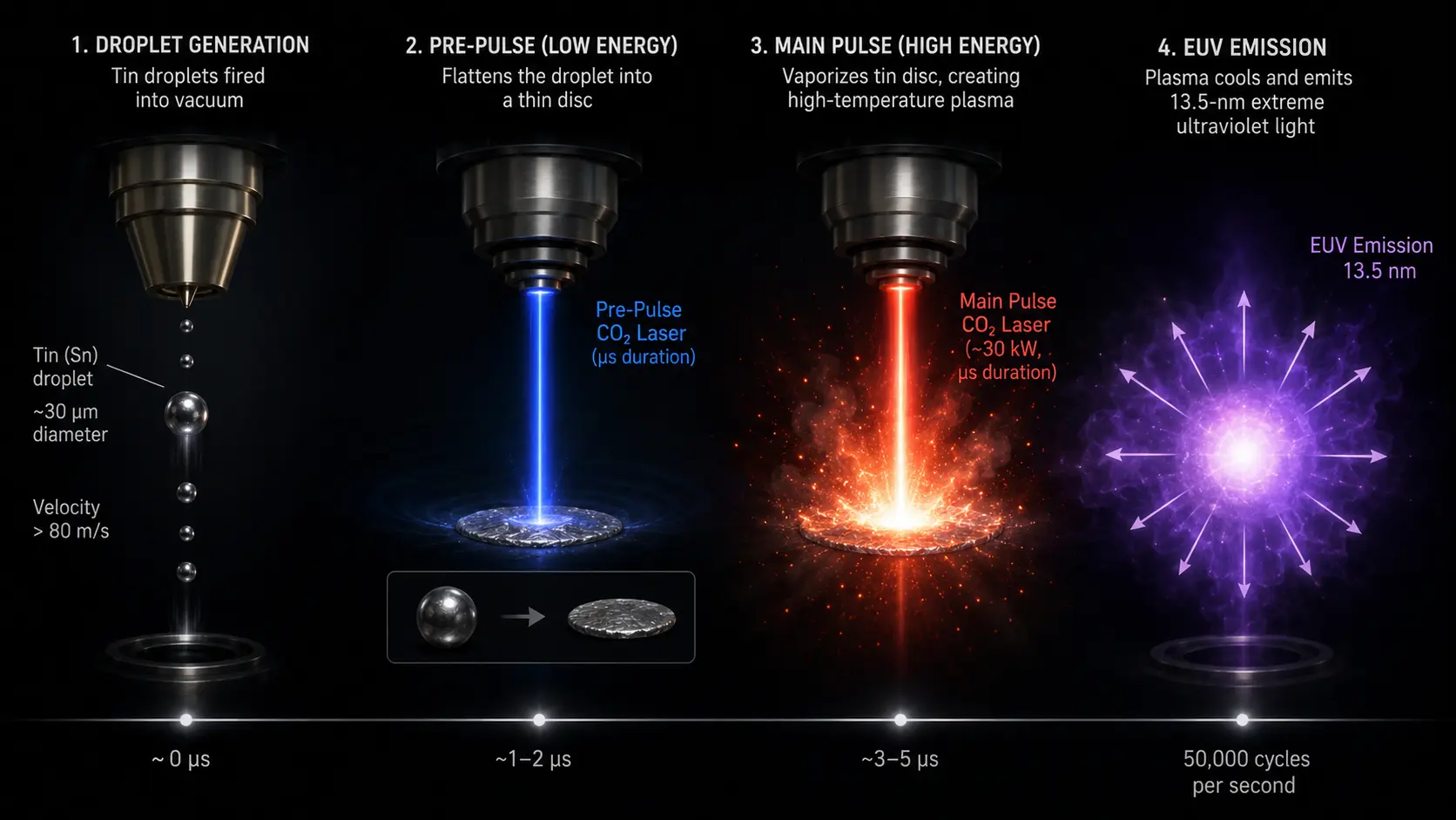
- Concept: Droplet Generation: A specialized nozzle fires microscopic droplets of liquid tin into a pure vacuum chamber at extreme velocity.
- Concept: The Pre-Pulse: A low-power laser strike flattens the spherical tin droplet into a pancake shape to maximize the target surface area.
- Concept: The Main Pulse: A 30-kilowatt carbon dioxide laser incinerates the flattened tin, forcing its electrons into a high-energy plasma state.
- Concept: 13.5-Nanometer Emission: As the plasma cools slightly, it violently emits extreme ultraviolet photons necessary for angstrom-level lithography.
HOW IT WORKS
Extreme ultraviolet (EUV) light does not exist naturally on Earth; it only occurs naturally in the coronas of stars. To print transistors smaller than a human virus, semiconductor foundries must create a miniaturized, contained star inside a vacuum chamber.
This artificial light generation occurs within the Laser-Produced Plasma (LPP) source. The process begins with a droplet generator shooting molten tin spheres, roughly thirty microns in diameter, into the vacuum chamber at velocities exceeding eighty meters per second.
As the tin droplet falls through the firing zone, a carbon dioxide (CO2) laser, typically manufactured by TRUMPF, executes a two-stage strike. The first strike is a low-energy pre-pulse. This pre-pulse does not destroy the tin; it imparts a shockwave that physically flattens the spherical droplet into a wider, thinner disc.
Microseconds later, the main 30-kilowatt CO2 pulse strikes this flattened disc. The laser energy instantly strips the electrons from the tin atoms, creating a dense, high-temperature plasma. The specific atomic structure of tin dictates that when this specific plasma relaxes, it emits photons exactly at the 13.5-nanometer wavelength required for advanced semiconductor lithography.
This entire sequence—droplet generation, pre-pulse flattening, main pulse vaporization, and photon emission—must occur exactly 50,000 times every single second to generate a continuous beam of usable EUV light.
WHY IT MATTERS NOW
The physical limit of computing power is currently bound by the conversion efficiency of this exact vaporization process. Foundries like TSMC and Intel require massive amounts of EUV light to expose silicon wafers fast enough to make high-volume chip manufacturing economically viable.
The LPP source is spectacularly inefficient. Less than five percent of the 30-kilowatt CO2 laser energy successfully converts into usable 13.5-nanometer light. The remaining 95 percent of the energy instantly turns into waste heat, scattered debris, and high-energy ions that violently attack the internal optics of the machine.
To transition from 3-nanometer to 2-nanometer and angstrom-era nodes, ASML is deploying High-NA (Numerical Aperture) scanners. These advanced machines require even more intense light, pushing the LPP source to output up to 600 watts of usable EUV power.
Generating this increased power requires shooting the tin droplets with even more aggressive laser strikes, exponentially increasing the sheer thermodynamic violence inside the vessel. Managing this plasma inferno requires hundreds of gallons of cooling water per minute and constant hydrogen gas flow to chemically sweep the vaporized tin off the delicate internal collector mirrors before the metal solidifies and blinds the optical system.
Mastering this physics problem dictates the timeline for next-generation artificial intelligence hardware. The inability to safely scale LPP source power without melting the internal optics is the primary mechanical bottleneck preventing the immediate mass production of denser neural network accelerators.
WHAT MOST PEOPLE MISS
Technology analysts track the delivery of ASML lithography machines as if they are standalone, self-contained printers. They miss the massive subterranean infrastructure required simply to fire the laser.
The 30-kilowatt CO2 laser does not fit inside the cleanroom scanner. It occupies an entire dedicated sub-fab floor located directly beneath the cleanroom. The laser beam must travel upward through a complex array of mirrors and vacuum tubes, actively maintaining a perfect sub-millimeter focal point on a microscopic, moving tin droplet fifty feet away.
Any microscopic building vibration—from a passing truck outside to the factory’s own air conditioning units—can throw the laser off target by a fraction of a micron. If the main pulse misses the direct center of the flattened tin pancake, the plasma formation fails, light output drops, and the multi-million-dollar silicon wafer sitting in the scanner above is permanently ruined by an underexposed circuit pattern.
THE TRAJECTORY
Next 12–36 Months: ASML will implement machine learning algorithms directly into the droplet tracking cameras. These neural networks will predict the microscopic kinematic drift of the falling tin, actively adjusting the pre-pulse laser steering mirrors in real-time to guarantee a perfect center strike on every droplet.
Next Five Years: Laser manufacturers will transition from CO2 architectures to advanced solid-state thulium lasers. These new pump sources operate at wavelengths that couple more efficiently with the tin plasma, increasing the total conversion efficiency from five percent to nearly ten percent, drastically reducing the electrical draw of the sub-fab infrastructure.
Next Ten Years: Free-electron lasers will emerge as a viable alternative for hyperscale foundries. Instead of firing individual lasers at tin inside every scanner, engineers will build massive, centralized particle accelerators that beam pure EUV light through vacuum pipes to multiple scanners simultaneously, completely eliminating the messy tin plasma process from the cleanroom floor.
What Could Go Wrong: If the hydrogen gas flow fails to chemically clean the primary collector mirror fast enough, microscopic layers of solid tin will accumulate on the reflective surface. Within hours, the mirror will absorb the laser energy instead of reflecting the EUV light, causing the massive optical element to violently crack under extreme thermal stress.
Most Likely Outcome: The tin-droplet laser-produced plasma source will remain the undisputed, unavoidable chokepoint for global logic scaling over the next decade. The sheer thermodynamic complexity of maintaining this continuous plasma state will restrict advanced node manufacturing to the very few firms capable of absorbing the extreme operational costs of LPP maintenance.
KEY TERMS
- Laser-Produced Plasma (LPP): A state of matter created by firing a high-power laser at a target material, instantly vaporizing it to generate specific wavelengths of light.
- Extreme Ultraviolet (EUV): An ultra-short wavelength of light (13.5 nanometers) used in advanced photolithography to print microscopic transistor geometries.
- Conversion Efficiency: The strict mathematical ratio comparing the amount of raw laser energy pumped into the tin droplet versus the amount of usable EUV light successfully generated.
- Collector Mirror: A massive, specialized optical element inside the source vessel that captures the omnidirectional EUV light emitted by the plasma and focuses it into the scanner.
- Pre-Pulse: An initial, low-power laser strike designed specifically to alter the physical geometry of a target droplet to maximize the absorption of the subsequent main laser strike.
SOURCES
- ASML — Extreme Ultraviolet (EUV) Light Source Architecture and Plasma Physics
- TRUMPF — High-Power CO2 Lasers for Laser-Produced Plasma Applications
- Applied Physics Letters — Tin Plasma Hydrodynamics and EUV Conversion Efficiency
- SPIE (International Society for Optics and Photonics) — Mitigation of Debris and Collector Mirror Degradation in LPP Sources