Advertisement
)
AT A GLANCE
- Concept: The Memory Wall: Individual GPUs possess immense processing power but very little onboard memory, starving them of data during large AI training runs.
- Concept: Unified Memory Architecture: NVLink allows any GPU in a server rack to directly read or write data to the memory of any other GPU without asking permission from a central processor.
- Concept: Switch Silicon: Rather than using standard copper cables, the fabric uses massive, dedicated silicon routing chips (NVSwitch) to manage the physical flow of data.
- Concept: The Interconnect Moat: Raw computing power is easily replicated by competitors; mastering the physical physics of high-speed data transfer across a data center is infinitely harder.
HOW THE NVLINK SWITCH FABRIC WORKS
Training a trillion-parameter artificial intelligence model like GPT-4 physically cannot occur on a single microchip. The neural network’s mathematical weights are far too large to fit into the High-Bandwidth Memory (HBM) of a single H100 or B200 Graphics Processing Unit (GPU).
Engineers must mathematically fracture the model, distributing its billions of parameters across thousands of separate GPUs in a technique called tensor parallelism. Because the model is split, the GPUs must constantly talk to each other to combine their fractional answers into a complete mathematical conclusion.
If these GPUs communicate using a standard computer motherboard connection (PCIe), the physical data transfer is disastrously slow. The GPUs will spend 90 percent of their time idling, waiting for the motherboard to deliver the data, completely negating the value of buying a $30,000 processor.
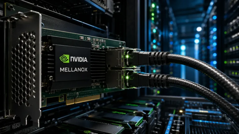
To bypass this physical bottleneck, Nvidia engineered NVLink. NVLink is a proprietary, point-to-point interconnect technology. It abandons the motherboard entirely, physically wiring the memory banks of multiple GPUs together using dense clusters of high-speed copper and optical links.
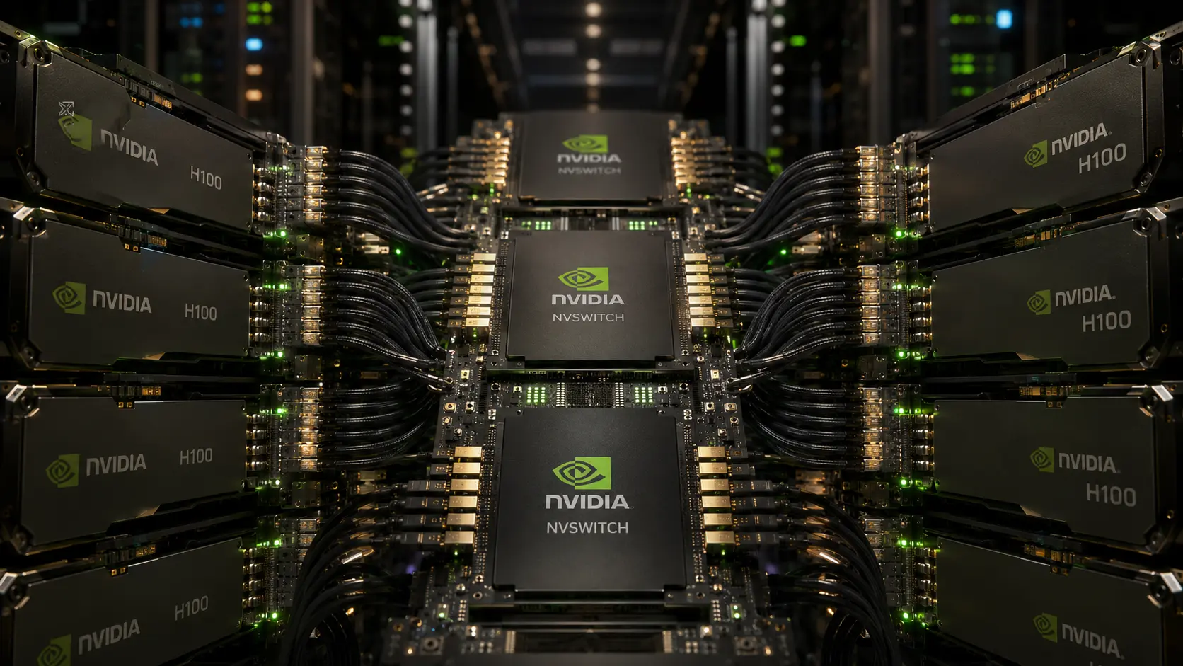
As cluster sizes expanded beyond a single server box, point-to-point wiring became mathematically impossible. Nvidia solved this by inventing the NVSwitch—a massive, custom silicon chip that acts as a central traffic cop. Instead of wiring every GPU to every other GPU, all GPUs wire into the NVSwitch fabric. This architecture allows an array of 576 separate GPUs to instantly share hundreds of terabytes of memory at speeds exceeding 1.8 terabytes per second, functionally fusing them into one singular, logically unified mega-GPU.
WHY IT MATTERS NOW
The generative AI arms race is fundamentally an exercise in data center networking physics. While companies like AMD and Intel design highly competitive, exceptionally fast individual processor chips, they mathematically fail to capture hyperscale market share.
This failure stems from the interconnect. Building a fast chip is a solvable physics problem. Networking 100,000 fast chips together without the entire cluster locking up in a traffic jam is an entirely different engineering discipline. Nvidia effectively monopolized the AI industry not just by building processors, but by building the NVLink Switch Fabric that glues them together.
Cloud providers like AWS, Google, and Meta are forced to buy the entire Nvidia ecosystem. If they attempt to mix Nvidia GPUs with cheaper, standard Ethernet networking switches from a third party, the training algorithms suffer severe latency penalties, causing multi-million dollar training runs to drag on for extra months.
Nvidia weaponized this dependency by integrating the NVLink routing logic directly into their hardware. The NVSwitch fabric possesses its own native mathematical processors that execute specific AI aggregation tasks (like “all-reduce” operations) in transit, before the data even reaches the destination GPU. This creates a deeply integrated, proprietary hardware ecosystem that competitors physically cannot replicate by simply designing a faster standalone microchip.
WHAT MOST PEOPLE MISS
Financial analysts consistently value semiconductor companies based on their ability to shrink transistors on a silicon wafer (Moore’s Law). They completely miss that the physical power consumption of the network is rapidly eclipsing the power consumption of the processor itself.
Pushing petabytes of data through copper NVLink cables across a massive server rack requires immense electrical voltage. The physics of electrical resistance means that transmitting data over distances greater than a few feet generates catastrophic thermodynamic heat. Hyperscale data centers are physically melting not because the GPUs are hot, but because the copper interconnect fabric required to feed them is reaching its absolute thermal limit.
THE TRAJECTORY
Next 12–36 Months: The transition from electrical NVLink to optical NVLink. To build clusters exceeding 100,000 GPUs, Nvidia and its competitors will replace dense copper cables with co-packaged optics (CPO). Microscopic lasers will beam the memory data across the NVSwitch fabric, drastically reducing electrical resistance, slashing power consumption, and allowing server racks to be spread further apart within the data center.
Next Five Years: The rise of Universal Chiplet Interconnect Express (UCIe). A massive coalition of competitors (including AMD, Intel, and Google) will finalize an open-source, standardized silicon interconnect to break Nvidia’s proprietary grip. This open standard will allow cloud providers to physically snap an AMD processor onto an Intel substrate and route memory between them seamlessly, commoditizing the interconnect layer.
Next Ten Years: Wafer-Scale Integration. Rather than cutting silicon into individual chips and attempting to network them back together with switches, companies like Cerebras will successfully manufacture singular, massive plates of continuous silicon. By keeping the entire neural network physically contained on one unbroken piece of glass, the need for external network switches and cables is entirely eliminated.
What Could Go Wrong: Advanced packaging constraints at TSMC. The NVSwitch silicon chips are massive, complex pieces of logic that require the exact same advanced 3D packaging (CoWoS) as the GPUs themselves. If TSMC experiences a supply chain bottleneck in its packaging facilities, Nvidia will mathematically be unable to manufacture the switches required to network the GPUs they have already produced, instantly stranding billions of dollars of un-networked silicon.
Most Likely Outcome: The interconnect fabric will completely consume the identity of the data center. Individual servers and standalone computers will cease to exist conceptually. The entire facility—encompassing hundreds of thousands of processors and exabytes of memory—will act and be programmed strictly as a single, liquid computational entity bound entirely by its optical networking limits.
KEY TERMS
- NVLink: A proprietary, high-speed, direct GPU-to-GPU interconnect technology developed by Nvidia to bypass standard motherboard bottlenecks.
- NVSwitch: A highly specialized silicon routing chip that connects multiple NVLink connections together, allowing massive arrays of GPUs to share memory.
- High-Bandwidth Memory (HBM): Specialized RAM physically stacked directly next to the processor core to provide massive data throughput required for AI.
- Tensor Parallelism: An algorithmic technique used to fracture a massive neural network across multiple physical processors to distribute the computational load.
- Co-Packaged Optics (CPO): An advanced hardware architecture where fiber-optic lasers are built directly into the silicon substrate to replace traditional copper electrical wires.
SOURCES
- Institute of Electrical and Electronics Engineers (IEEE) — High-Performance Interconnects and the Evolution of the NVSwitch Architecture
- Nvidia Corporation — NVLink and NVSwitch System Architecture Technical Whitepapers
- Next Platform — The Physics of Hyperscale AI Networking and the Memory Wall
- Semiconductor Research Corporation (SRC) — Co-Packaged Optics and the Thermal Limits of Copper Interconnects