Advertisement
)
AT A GLANCE
- Concept: The Organic Limit: Traditional plastic substrates warp and bend under extreme heat, permanently severing microscopic silicon connections.
- Concept: Through-Glass Vias: Lasers drill millions of perfectly straight, micrometer-wide holes through a solid glass plate to route electrical signals.
- Concept: Thermal Dissipation: Glass withstands vastly higher temperatures than plastic, allowing chipmakers to push higher voltages into AI accelerators.
- Concept: Dimensional Stability: Because glass does not shrink or expand unevenly, engineers can pack transistors infinitely closer together without physical misalignment.
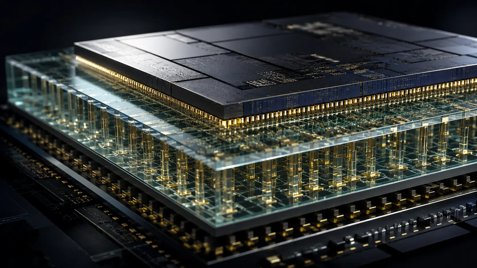
HOW IT WORKS
A modern microchip does not plug directly into a computer motherboard. It sits on a structural interposer known as a substrate. This foundational layer acts as a physical translator, taking the microscopic electrical signals from the silicon die and routing them outward to the macroscopic metal pins of the main circuit board.
For twenty years, these substrates were manufactured from organic epoxy resins. As chips process heavy computational workloads, they generate extreme thermodynamic heat. This heat causes the organic plastic to warp, bend, and physically swell. This dimensional instability physically snaps the fragile, micrometer-scale solder bumps connecting the silicon to the board, destroying the processor.
To solve this physical limitation, manufacturers are replacing plastic with ultra-pure fused silica glass. Glass provides absolute mechanical rigidity and perfect flatness at a microscopic level. It does not warp under extreme thermal stress. To move electricity through this impenetrable barrier, engineers utilize femtosecond lasers to bore millions of microscopic holes, a process known as creating Through-Glass Vias (TGVs).
After laser drilling, chemical vapor deposition fills these tiny glass tunnels with highly conductive copper. The smooth, inorganic walls of the glass allow for mathematically perfect metal plating without internal voids.
Because glass is a superior electrical insulator compared to plastic, these copper channels suffer nearly zero signal leakage or capacitance loss. Data travels at significantly higher frequencies without electromagnetic cross-talk. This specific material property feeds data-hungry artificial intelligence processors at speeds that organic materials physically cannot support.
WHY IT MATTERS NOW
The artificial intelligence boom has pushed baseline silicon design to its absolute thermodynamic breaking point. A single high-end AI accelerator now consumes over a thousand watts of electricity. Pumping this extreme voltage through legacy organic substrates rapidly degrades the material, placing a hard physical cap on the maximum power a data center can safely push into a chip.
Because chipmakers can no longer easily shrink individual transistors to improve performance, they must build vertically. The industry is rapidly adopting 3D stacking, placing multiple logic and memory dies directly on top of each other. This three-dimensional architecture requires a mathematically perfect, flat foundation. If an organic substrate bows even a fraction of a millimeter during manufacturing, the entire billion-dollar wafer becomes useless scrap.
Glass substrates physically solve this mechanical alignment problem. They allow chip designers to construct massive, multi-die “chiplets” that operate seamlessly as a single logical processor. This innovation physically shifts the primary bottleneck of AI computation away from TSMC’s silicon foundries and places it directly onto the advanced packaging facilities building these glass foundations.
The transition to glass dictates billions of dollars in fresh global capital expenditure. Chemical companies and hardware manufacturers are aggressively financing the first commercial glass substrate factories to meet expected demand. The supply chain for advanced packaging is being completely rewritten in real-time.
The nation that masters the optical drilling and metallization of glass will secure absolute control over the next decade of hardware infrastructure. Controlling the substrate mathematically equates to controlling the physical limits of planetary computation.
WHAT MOST PEOPLE MISS
Mainstream hardware analysts focus entirely on how glass improves copper wire routing density. They completely miss the inherent optical properties of the material itself. Because the substrate is literally constructed from fused silica, engineers can embed silicon photonics directly into the foundation of the chip.
Instead of forcing electrons through copper wires, future AI chips will shoot microscopic lasers directly through the glass substrate to communicate with adjacent server racks. This architecture completely bypasses the thermodynamic heat generated by traditional electrical resistance.
The true value of a glass core is not just holding silicon perfectly flat to prevent warping. The unstated endgame is utilizing the glass as a physical medium for light-based, zero-latency computing, structurally erasing the data transfer bottlenecks of modern hyperscale data centers.
THE TRAJECTORY
Next 12–36 Months: Major semiconductor manufacturers will activate low-volume commercial production of glass core substrates strictly for high-margin data center processors. Early factory yields will remain mathematically poor due to the physical fragility of handling ultra-thin glass panels on fast, automated assembly lines.
Next Five Years: Through-Glass Via drilling will shift from mechanical etching to advanced laser-induced deep etching (LIDE). This optical technique will exponentially increase manufacturing throughput, rapidly dropping the unit cost of glass substrates to parity with high-end organic equivalents.
Next Ten Years: The physical limit of copper electrical signaling will force the complete integration of co-packaged optics. Glass substrates will act as microscopic, integrated fiber-optic networks, routing laser data directly into the silicon logic gates to power exascale quantum and AI data centers.
What Could Go Wrong: Glass is inherently brittle and highly susceptible to microscopic stress fractures. If robotic handlers in the cleanroom accidentally induce a micro-fracture during the metallization phase, the entire panel will spontaneously shatter during the high-temperature solder reflow process, instantly destroying thousands of dollars of attached silicon dies.
Most Likely Outcome: Organic substrates will remain the standard foundation for cheap consumer electronics and mobile devices. However, glass cores will become the mandatory physical baseline for all high-performance, high-wattage silicon, forcing the advanced packaging industry to transition from plastics manufacturing to precision optical engineering.
KEY TERMS
- Through-Glass Via (TGV): A microscopic vertical tunnel laser-drilled through a glass substrate and filled with conductive metal to route electrical signals.
- Advanced Packaging: The final manufacturing phase where multiple separate microchips are vertically stacked and wired together into a single, high-density functional unit.
- Organic Substrate: The legacy plastic and epoxy-based foundation that currently holds microchips, highly prone to warping and expansion under high thermal loads.
- Silicon Photonics: The engineering discipline that replaces traditional copper electrical wires with microscopic lasers and fiber-optic channels built directly into a semiconductor.
- Chiplet: A modular, independently manufactured piece of silicon designed to be physically combined with other chiplets on a single substrate to form a larger, unified processor.
SOURCES
- Institute of Electrical and Electronics Engineers (IEEE) — Through-Glass Via (TGV) Technology and High-Density Advanced Packaging
- Intel Corporation — Glass Substrates for Next-Generation Advanced Packaging and Scaling
- Georgia Institute of Technology — Packaging Research Center Studies on Dimensional Stability of Fused Silica Cores
- Semiconductor Research Corporation (SRC) — Thermal and Electrical Characteristics of Post-Organic Substrate Materials