Advertisement
)

AT A GLANCE
- Concept: IR Drop: The mathematical loss of electrical voltage caused by resistance in microscopic copper wires.
- Concept: Front-Side Routing: The legacy architecture forcing both power and data through the top of the chip.
- Concept: Wafer Thinning: Physically grinding away the bottom of the silicon crystal to expose the transistor roots.
- Concept: Nano-TSV: Microscopic vertical copper tunnels drilled upward to feed electricity directly into the transistor source.
HOW BACKSIDE POWER DELIVERY WORKS
For sixty years, semiconductor foundries built microchips like city blocks layered entirely from the top down. Engineers printed the silicon transistors on the ground floor, then stacked over fifteen layers of microscopic copper wiring directly above them. This complex metal canopy had to handle two distinct jobs simultaneously: transmitting data signals and delivering raw electrical power.
As transistors shrank below the 3-nanometer threshold, this dual-purpose canopy became physically untenable. Forcing electrical current through miles of increasingly narrow top-layer copper wires generates massive electrical resistance. This resistance causes a severe IR voltage drop, meaning the electricity physically loses its power before it ever reaches the transistors at the bottom.
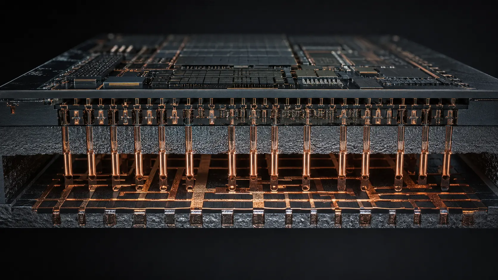
To bypass this geometric bottleneck, foundries developed the Backside Power Delivery Network (BSPDN). Engineers completely separate the power wires from the data wires by physically flipping the silicon wafer upside down mid-production. They use industrial grinders to shave away the thick, unused silicon at the bottom of the chip, exposing the bare undersides of the transistors.
Once the foundry exposes the transistor roots, machines drill millions of nano-Through-Silicon Vias (nTSVs) straight upward. They fill these microscopic vertical tunnels with copper, connecting a brand-new, dedicated power grid directly to the transistor source contacts. The data signals remain on the top of the chip, while pure, uninterrupted electricity flows freely from the bottom.
WHY IT MATTERS NOW
The global artificial intelligence race currently faces an absolute physical speed limit dictated by voltage starvation. Frontier AI accelerators, like those powering massive large language models, require up to 1,000 watts of continuous power to calculate their math. If the electrical current experiences a ten percent IR drop traveling through legacy front-side wiring, the processor mathematically stalls and fails to complete the computation.
Backside power delivery physically solves this exascale computing crisis. By feeding electricity through wide, low-resistance copper tracks on the bottom of the die, the nTSVs deliver maximum voltage directly to the logic gates. This single architectural shift instantly increases transistor switching speeds by up to six percent without requiring any changes to the underlying transistor chemistry.
Intel staked its entire corporate turnaround on mastering this specific physical inversion, branding its proprietary version as PowerVia. By successfully integrating backside power on its Intel 20A node before its Taiwanese rivals, Intel aims to reclaim the undisputed performance crown in global semiconductor manufacturing.
The financial implications stretch entirely across the global semiconductor supply chain. Moving the power grid to the backside frees up massive physical real estate on the front side of the chip. Foundries use this newly empty space to route data signals more efficiently, allowing chip designers to pack thirty percent more transistors into the exact same silicon footprint.
WHAT MOST PEOPLE MISS
Hardware enthusiasts frequently assume that extreme wafer thinning is a simple mechanical sanding process. They completely miss the brutal thermal-mechanical stress involved in grinding a 300-millimeter silicon wafer down to just a few hundred nanometers thick. At this extreme thinness, the silicon crystal becomes as flexible and fragile as plastic wrap, immediately warping or shattering under its own internal stress.
To prevent the wafer from snapping during the flip, foundries must bond the active silicon to a temporary glass carrier wafer using advanced organic adhesives. The true manufacturing moat lies in the chemical debonding process. If the factory cannot perfectly un-glue the finished chip from the glass carrier without leaving microscopic residue, the entire batch of AI processors fails physical inspection, driving factory yields to zero.
THE TRAJECTORY
Next 12–36 Months: Major foundries will scale their initial backside power nodes to commercial volume. Fabless designers will rewrite their entire electronic design automation (EDA) software suites to accommodate routing power and signals on opposite sides of the die.
Next Five Years: The integration of buried power rails into standard logic architectures. Engineers will bury thick metallic power lines directly inside the shallow trench isolation oxide between transistors, acting as local power substations fed instantly by the underlying nTSVs.
Next Ten Years: The realization of active backside components. Foundries will stop using the backside purely for power delivery and begin printing entire secondary layers of memory and voltage-regulating capacitors directly underneath the logic transistors, creating true monolithic 3D computation.
What Could Go Wrong: Severe thermal runaway. Top-side copper wiring historically acts as an excellent passive heat sink. Removing these dense power wires from the front side physically traps the heat inside the logic layer, requiring vastly more complex liquid cooling systems to prevent the processor from melting.
Most Likely Outcome: Backside power delivery will become the mandatory architectural standard for all high-performance computing. The basic physics of copper resistance guarantee that sub-2nm scaling mathematically requires separating power from data to maintain stable operational voltages.
KEY TERMS
- Nano-Through-Silicon Via (nTSV): A microscopic vertical tunnel drilled into silicon and filled with metal to conduct electricity between different vertical layers.
- IR Drop: The mathematical reduction in electrical voltage that occurs naturally when current pushes through the physical resistance of a wire.
- Wafer Thinning: The mechanical and chemical grinding of a silicon crystal to reduce its physical thickness before advanced packaging.
- Buried Power Rail: A thick, highly conductive metal line embedded directly inside the silicon substrate to distribute local power to neighboring transistors.
- Back-End-Of-Line (BEOL): The final manufacturing stage where a foundry constructs the complex microscopic copper wiring canopy above the transistors.
SOURCES
- Intel Corporation — PowerVia: Intel’s Backside Power Delivery Architecture
- Imec — Backside Power Delivery Networks and Nano-TSV Integration
- Institute of Electrical and Electronics Engineers (IEEE) — IR Drop Mitigation in Sub-2nm Nodes via Buried Power Rails
- TSMC Open Innovation Platform — N2 Technology and Backside Routing Performance