Advertisement
)

AT A GLANCE
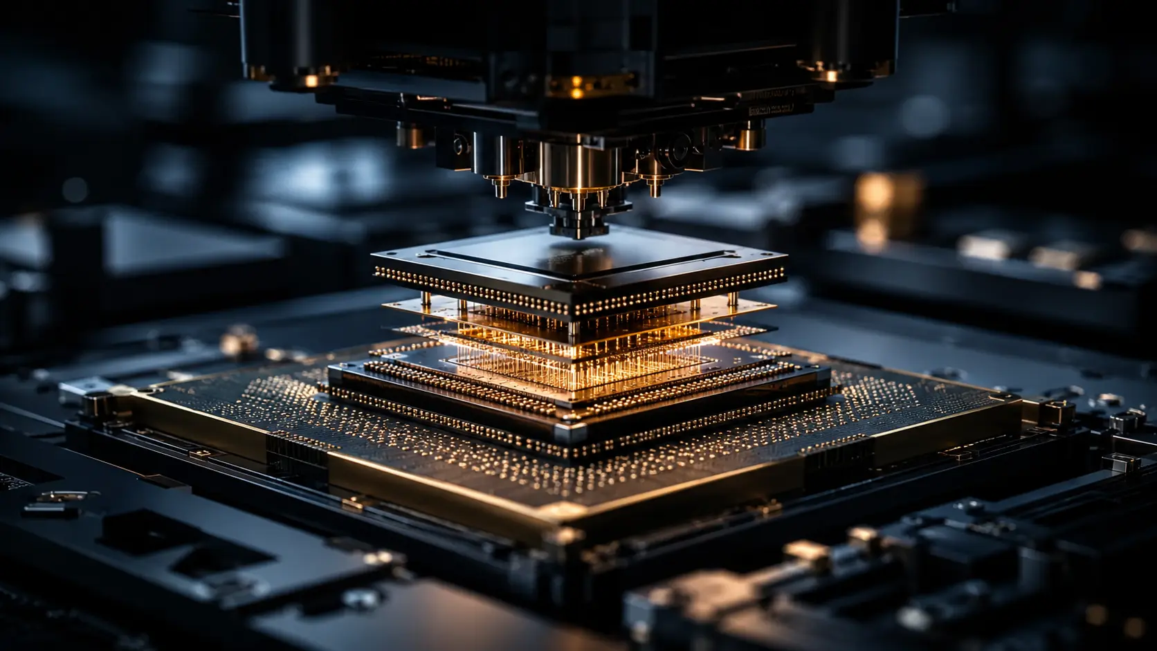
- Concept: Advanced Packaging: Connecting multiple microscopic silicon chips together into a single, high-density 3D stack.
- Concept: OSAT Industry: Third-party factory networks that handle the physical packaging and testing of chips for major design companies.
- Concept: Fan-Out Wafer-Level Packaging (FOWLP): A technique that expands the available connection area of a chip to allow more data pathways.
- Concept: Thermal Interface Material (TIM): Highly specialized chemical compounds used to transfer immense heat away from densely stacked processors.
IN SIMPLE WORDS
Printing a microchip is like manufacturing the engine of a supercar. It is incredibly complex and expensive. But a bare engine sitting on a factory floor cannot drive. It needs a chassis, a cooling system, and complex wiring to connect it to the steering wheel.
In the semiconductor world, this final construction phase is called packaging. For decades, packaging was an afterthought—a cheap plastic shell glued around a chip to protect it from dust.
Today, artificial intelligence chips are too massive to print in one piece. Instead, companies print dozens of smaller chips and send them to specialized factories called OSATs. These factories act as microscopic architects. They stack the tiny chips on top of each other, wire them together with connections thinner than a human hair, and pack them in heat-absorbing gel. Without this advanced assembly process, the fastest chips in the world are completely useless pieces of raw silicon.
HOW ADVANCED PACKAGING WORKS
The traditional semiconductor supply chain consisted of three silos: chip designers, wafer foundries, and packaging facilities. Outsourced Semiconductor Assembly and Test (OSAT) companies historically performed the low-margin back-end work. They received finished silicon wafers, sliced them into individual squares (dies), attached a few wire bonds, and encased them in black plastic.
Advanced computing destroyed this simple model. The physical limitations of Moore’s Law forced the industry to adopt chiplet architecture. Because massive processors cannot be printed flawlessly on a single silicon die, foundries print multiple smaller, specialized chiplets. These raw pieces must be fused together perfectly to function as one unified brain.
This requires Wafer-Level Chip-Scale Packaging (WLCSP). Instead of cutting the wafer and packaging the chips individually, OSAT facilities perform the packaging steps while the chips are still bound together on the original circular silicon wafer. This allows for microscopic, photolithographic precision when placing copper connection pillars.
To expand data bandwidth, OSATs utilize Fan-Out Panel-Level Packaging (FOPLP). When a chip is too small to fit the thousands of electrical connections it needs, engineers embed the bare chip into a larger artificial mold. They then “fan out” the microscopic wiring beyond the physical edge of the silicon chip into the surrounding mold. This creates a much larger surface area to attach massive arrays of high-speed solder bumps.
The physical assembly process requires extreme kinetic precision. Robotic pick-and-place arms must align microscopic copper pillars between two stacked chips with sub-micron accuracy, executing this alignment in milliseconds. If the placement is misaligned by a fraction of a degree, the electrical connection fails, and the entire multi-thousand-dollar assembly is thrown away.
Once connected, the 3D stack generates extreme thermal density. Multiple high-performance chips stacked vertically will melt each other if not managed properly. OSAT engineers inject highly specialized Thermal Interface Materials (TIM) between the silicon layers and the external heat spreaders to aggressively pull heat out of the core, ensuring the logic chips survive operation.
REAL WORLD EXAMPLE
Nvidia’s absolute dominance in artificial intelligence is entirely dependent on advanced packaging. Nvidia does not manufacture its own H100 or Blackwell chips. They contract Taiwan Semiconductor Manufacturing Company (TSMC) to print the raw silicon.
However, printing the chips is only half the battle. TSMC also controls the proprietary CoWoS (Chip-on-Wafer-on-Substrate) packaging technology. This specific assembly technique physically glues the Nvidia logic processor to six stacks of High-Bandwidth Memory (HBM). Because TSMC is one of the only companies on Earth that can execute this complex packaging at scale, Nvidia’s output is strictly capped by TSMC’s monthly packaging capacity, not its silicon printing capacity.
WHY IT MATTERS NOW
Advanced packaging has officially replaced silicon lithography as the ultimate chokepoint in the global computing supply chain. For twenty years, nations fought to acquire the extreme ultraviolet (EUV) lithography machines required to print the smallest transistors.
Today, even if a country prints a perfect 3-nanometer chip, it cannot build an AI supercomputer without advanced packaging. The ability to physically stack and wire diverse chiplets onto a silicon interposer dictates the final speed and power efficiency of the processor.
The OSAT industry is heavily concentrated in Southeast Asia. Taiwan controls the high-end advanced packaging market through foundries like TSMC, while companies like ASE Technology (Taiwan) and Amkor (USA/South Korea) dominate the broader outsourced market. Malaysia currently handles roughly 13 percent of the world’s back-end testing and traditional packaging.
This creates a terrifying geopolitical vulnerability for Western nations. The United States passed the CHIPS Act to bring raw silicon printing back to American soil. However, if an American foundry prints a wafer in Arizona, but must still ship that wafer on a cargo plane to Malaysia or Taiwan to be sliced, packaged, and tested, the supply chain remains fundamentally broken.
Without domestic OSAT facilities, billion-dollar onshore fabrication plants are essentially building highly expensive, unfinished puzzle pieces that cannot be used by the military or civilian tech sectors until they cross the Pacific Ocean twice.
COMMON MISCONCEPTIONS
- “Packaging is just putting a plastic box around a chip.” This was true in 1995. Today, advanced packaging is a microscopic engineering discipline involving chemical bonding, laser drilling, and silicon routing that is nearly as complex as printing the chip itself.
- “Only OSAT companies do packaging.” The lines are blurring. Massive foundries like TSMC and Intel are aggressively building their own in-house advanced packaging divisions to capture the high profit margins of 3D stacking.
- “Advanced packaging makes chips cheaper.” It actually makes the final assembled product much more expensive and difficult to manufacture. It is used because printing one giant monolithic chip is no longer physically possible without massive failure rates.
WHAT MOST PEOPLE MISS
Supply chain analysts focus heavily on the robotic placement machines, but they frequently overlook the massive shortage of ABF substrates.
Ajinomoto Build-up Film (ABF) is a highly specialized insulation resin used to build the foundational layers beneath the packaged chip. It routes the microscopic wires from the silicon down to the larger motherboard. The global supply of ABF is controlled by a tiny handful of Japanese chemical companies. If these obscure chemical suppliers experience a production hiccup, the entire global OSAT industry instantly halts, paralyzing global server production.
THE ECONOMIC AND STRATEGIC IMPACT
The primary financial beneficiaries of this transition are the tier-one OSAT providers and the specialized equipment manufacturers that build the high-speed placement and testing robotics. Companies that historically suffered from low profit margins are seeing their valuations skyrocket as packaging transitions from a commodity service to a highly guarded proprietary technology.
Strategically, advanced packaging offers a powerful loophole for nations facing severe export controls. If a nation is banned from buying the machinery required to print ultra-advanced 3-nanometer chips, they can compensate by using advanced packaging. They can cheaply print dozens of older, bulkier 14-nanometer chips domestically, and use advanced 3D packaging to stack them together. This creates a composite mega-chip that rivals the processing power of the restricted technology.
For investors, the substrate and chemical suppliers that feed the OSAT industry represent the ultimate hidden monopolies. Securing the capacity for advanced glass substrates and thermal gels dictates who wins the race to build the next generation of data centers.
THE TRAJECTORY
Next 12–36 Months: The rapid expansion of panel-level packaging. Instead of packaging chips on 300-millimeter circular wafers, OSATs will adopt massive rectangular glass panels. This will allow them to package four times as many chips simultaneously, drastically lowering assembly costs and easing the current AI bottleneck.
Next Five Years: The rise of hybrid bonding. OSATs will stop using microscopic solder bumps to connect layers of silicon. Instead, they will polish the silicon surfaces so perfectly flat that the copper connections permanently fuse together at room temperature. This will allow components to be stacked mere micrometers apart, virtually eliminating data latency.
Next Ten Years: The integration of silicon photonics in the package. OSAT facilities will embed microscopic optical lasers directly inside the chip packaging. The packaged processors will communicate with each other using light instead of electricity, breaking the thermodynamic limits of modern data centers.
What Could Go Wrong: A catastrophic geographical disruption. Because the OSAT industry requires massive amounts of clean water and highly stable electricity, severe droughts or power grid failures in Taiwan or Malaysia would instantly choke the global supply of finished electronics, causing immediate price spikes in everything from automobiles to smartphones.
Most Likely Outcome: Advanced packaging will become the primary battleground for semiconductor supremacy. Western nations will be forced to heavily subsidize domestic OSAT infrastructure to close the loop on their semiconductor supply chains, ensuring that raw silicon printed locally can actually be assembled and utilized locally.
KEY TERMS
- OSAT (Outsourced Semiconductor Assembly and Test): Third-party companies that specialize in taking raw silicon wafers and physically packaging them into finished microchips.
- Advanced Packaging: The complex process of vertically stacking and connecting multiple specialized silicon chips into a single, high-performance unit.
- Chiplet: A small, specialized piece of silicon designed to be physically wired to other chiplets inside an advanced package.
- Fan-Out Packaging: A technique that embeds a chip in a larger mold to expand the physical area available for external electrical connections.
- Hybrid Bonding: A next-generation connection technique that directly fuses copper pads on different chips together without using solder.
- Thermal Interface Material (TIM): Chemical pastes or liquid metals injected into a chip package to pull destructive heat away from the silicon.
BEGINNER FAQ
What does an OSAT company do? They do the physical assembly. A company like Apple designs a chip, a factory prints it on a silicon disc, and an OSAT company cuts it out, wires it up, and puts it in a protective case.
Why is packaging suddenly so important? Because chips have gotten too big to print in one piece. We now have to print them in smaller pieces and glue them together. If the gluing and wiring aren’t perfect, the chip doesn’t work.
What is 3D stacking? Instead of placing chips flat next to each other, engineers stack them vertically like a skyscraper. This saves space and lets data travel between the chips much faster.
Why is heat a problem in advanced packaging? When you stack multiple powerful computer chips directly on top of each other, the heat gets trapped in the middle. If the packaging company does not use advanced cooling gels, the chips will melt.
Where are these OSAT factories located? The vast majority of them are located in Asia, specifically in Taiwan, Malaysia, South Korea, and China.
Why doesn’t the United States do this? Historically, packaging was considered low-skill, low-profit work, so Western companies outsourced it to Asia to save money. Now that it is highly complex and critical to AI, the US is struggling to rebuild those factories.
What is a chiplet? A chiplet is like a single LEGO brick. By itself, it only does one thing (like memory or math). Advanced packaging is the process of snapping dozens of chiplets together to build a complete processor.
Can any factory do advanced packaging? No. It requires extreme precision, microscopic robotics, and hyper-clean environments. Only a handful of companies globally have the technology to package the highest-end AI chips.
SOURCES
- Semiconductor Equipment and Materials International (SEMI) — Global OSAT Manufacturing and Advanced Packaging Trends
- Institute of Electrical and Electronics Engineers (IEEE) — Fan-Out Wafer-Level Packaging and Hybrid Bonding Architecture
- Semiconductor Industry Association (SIA) — The Semiconductor Supply Chain and Domestic Assembly Vulnerabilities
- Taiwan Semiconductor Manufacturing Company (TSMC) — 3DFabric and Advanced Chiplet Integration