Advertisement
)

At a Glance
- Concept: Growing flawless diamonds atom-by-atom from a superheated gas plasma.
- Why it matters: Diamonds are critical for drilling, cutting, and heat management in modern electronics; lab-grown variants bypass the ethical and economic constraints of the global mining cartel.
- Who uses it: Semiconductor foundries, aerospace contractors, heavy industrial manufacturers, and quantum computing labs.
- Biggest takeaway: Synthetic CVD diamonds are not “fake”; they are physically, chemically, and optically identical to mined diamonds, but can be customized with extreme precision for electronic superiority.
In Simple Words
Most people think of diamonds as expensive jewelry dug out of the earth. But to a physicist, a diamond is simply carbon atoms arranged in a highly specific, rigid grid. This grid makes diamond the hardest physical material in the universe and the single best conductor of heat. We need millions of carats of diamonds to drill through solid rock for oil, to polish silicon microchips, and to cut hardened steel.
Historically, we had to rely on a massive global mining cartel to supply these stones. Today, we make them in a laboratory.
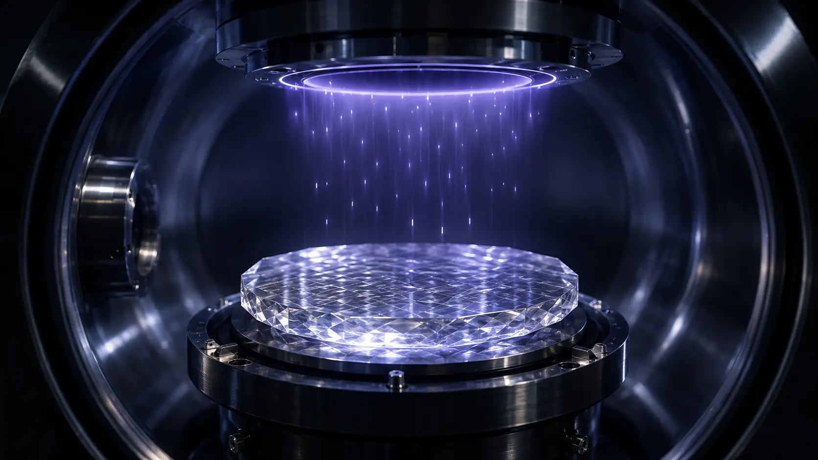
Using Chemical Vapor Deposition (CVD), scientists take a microscopic “seed” of a diamond and place it in a vacuum chamber. They fill the chamber with methane gas and blast it with high-power microwaves until the gas turns into a blazing plasma, hotter than the surface of the sun. The intense energy breaks the gas apart, causing raw carbon atoms to rain down and lock onto the seed, growing a perfect diamond layer by layer. We are no longer mining diamonds; we are printing them from hot gas.
Why This Matters
The global synthetic diamond market has reached massive proportions, valued at roughly $28.6 billion in 2026. While consumer jewelry captures the headlines, the true economic engine is the industrial sector.
Mined diamonds are fundamentally unpredictable. They contain natural defects, trapped nitrogen, and structural flaws that make them highly unreliable for extreme-precision engineering. As global manufacturing pivots to electric vehicles (EVs), deep-space optics, and ultra-high-power radar, standard silicon microchips overheat and melt. Diamond is the ultimate heat sink. It conducts heat five times better than copper.
Furthermore, the traditional diamond supply chain is deeply flawed. The Kimberley Process was established to prevent the trade of “blood diamonds” funding armed conflicts, but it has historically struggled with opaque tracing and enforcement. By synthesizing diamonds domestically, nations instantly secure a flawless, ethical, and strategically infinite supply of the world’s most critical super-material, completely neutralizing the geopolitical leverage of legacy mining monopolies.
The Big Picture
The transition from mined diamonds to CVD diamonds represents the shift from resource extraction to advanced manufacturing.
For decades, the only way to make an artificial diamond was the High Pressure High Temperature (HPHT) method, which required massive hydraulic presses to physically crush carbon with millions of pounds of force. HPHT was excellent for creating cheap, gritty diamond powder for sandpaper and saw blades, but it produced flawed, yellow-tinted crystals unsuitable for modern electronics.
CVD changes the paradigm entirely. It operates at low pressures. It does not crush carbon; it gracefully deposits it. This allows engineers to grow massive, pure, single-crystal diamond wafers that are completely transparent to infrared lasers and immune to high-voltage electrical blowouts.
HOW PRINTED DIAMONDS WORK
Growing a crystal lattice from a vacuum requires manipulating the fundamental thermodynamic states of carbon.
1. The Fundamental Problem
A diamond is simply carbon crystallized in a 3D tetrahedral lattice. However, under normal atmospheric conditions, carbon naturally prefers to organize itself into flat, slippery sheets (graphite, like the lead in a pencil). The fundamental challenge of synthetic diamond manufacturing is forcing carbon atoms to abandon their preferred graphite state and adopt the highly pressurized, rigid structure of a diamond without actually using physical pressure.
2. The Insufficiency of HPHT
Early synthetic methods used High Pressure High Temperature (HPHT) machines. They replicated the center of the Earth, using giant hydraulic anvils to crush graphite at 1.5 million pounds per square inch. While successful, the extreme physical forces made it impossible to grow wide, flat, continuous wafers necessary for semiconductor manufacturing. HPHT machines also inadvertently trapped metal catalysts inside the diamond, ruining its optical clarity and electrical resistance.
3. The Core Mechanism of CVD
Chemical Vapor Deposition solves this by using chemical energy instead of physical pressure. A thin slice of a natural or lab-grown diamond, known as a “seed,” is placed inside a vacuum chamber. The chamber is flooded with a mixture of hydrogen and methane gas. Microwaves are fired into the chamber, igniting the gas into a glowing ball of superheated plasma. The intense energy breaks the methane molecules apart, freeing the carbon atoms. These carbon atoms rain down and attach themselves to the diamond seed, continuing its exact crystalline pattern.
4. Technical Depth: Epitaxial Growth and Atomic Hydrogen
This process is called homoepitaxial growth. The secret to preventing the carbon from turning into useless graphite lies in the hydrogen gas. Inside the microwave plasma, atomic hydrogen acts as a highly aggressive chemical janitor. Because graphite bonds are slightly weaker than diamond bonds, the atomic hydrogen instantly etches away any carbon atoms that try to form graphite on the surface, leaving only the perfect, unbreakable sp3 diamond bonds behind. This ensures the crystal lattice grows flawlessly, atom by atom.
5. Real-World Consequences: Semiconductor Substrates
Because the MPCVD (Microwave Plasma CVD) process occurs in a highly controlled vacuum, engineers can introduce trace gases to perfectly “dope” the diamond. Adding trace amounts of boron turns the diamond from an electrical insulator into a highly conductive, ultra-wide bandgap semiconductor. This enables the creation of diamond-based transistors capable of operating at extreme voltages and temperatures exceeding 500°C without requiring heavy cooling systems—a holy grail for electric vehicle powertrains.
Real-World Applications
The disruption of CVD reaches far beyond standard drill bits, empowering next-generation technologies.
High-Power Semiconductor Heat Spreaders: Traditional silicon microchips create immense heat. The diamond semiconductor market, projected to grow to over $1 billion by 2034, utilizes synthetic CVD diamond wafers directly beneath power-dense chips (like GaN RF amplifiers). The diamond pulls the heat away laterally, allowing military radar systems and 5G cellular towers to run at massive power levels without melting.
Extreme Deep-Hole Drilling: The oil, gas, and geothermal energy industries rely on Polycrystalline Diamond Compact (PDC) drill bits. Mined diamonds shatter under the extreme torsional stress of drilling through three miles of solid granite. CVD processes are used to coat tungsten carbide drill bits with a thick, uniform layer of synthetic diamond, creating self-sharpening abrasive tools that double the operational lifespan of heavy drilling rigs.
Laser Optics and Directed Energy Weapons: Pure CVD diamond is optically transparent from the ultraviolet spectrum deep into the infrared. Defense contractors use massive, lab-grown diamond windows to cap highly powerful industrial lasers and directed-energy weapons. Unlike glass or sapphire, the diamond window will not absorb the heat of the laser and shatter during continuous firing.
Economic & Strategic Impact
The widespread commercialization of MPCVD technology has fundamentally disrupted the historic diamond monopoly.
By 2026, the cost to synthetically print a flawless, one-carat diamond has plummeted below $300, while traditional mining conglomerates face increasing operational costs due to depleted geological reserves. This has permanently fractured the pricing model of the global diamond industry.
Strategically, the ability to domestically manufacture electronic-grade diamond wafers is now a matter of national security. Governments in the United States, Japan, and the EU are heavily subsidizing advanced materials foundries. Establishing a state-of-the-art MPCVD diamond wafer production line requires massive capital expenditure, frequently exceeding $500 million. However, controlling the supply chain for ultra-wide bandgap (UWBG) materials ensures dominance in next-generation quantum computing, hypersonic missile guidance, and EV efficiency grids.
Advantages
- Flawless Structural Purity: The vacuum environment of CVD ensures the diamond is free of nitrogen inclusions and structural deformities found in naturally mined stones.
- Extreme Thermal Conductivity: Achieves unmatched heat dissipation (exceeding 2,200 W/m·K), making it superior to silicon carbide (SiC) and gallium nitride (GaN) for thermal management.
- Ethical and Traceable Supply Chain: Eliminates the human rights abuses, ecological destruction, and opaque trading routes historically associated with diamond mining.
- Customizable Wafer Sizing: Unlike HPHT, which grows chunk-like stones, CVD can grow wide, flat, continuous discs perfectly tailored for semiconductor fabrication lines.
Limitations
- High Capital Expenditure: The microwave plasma reactors, high-purity methane, and ultra-high-vacuum equipment require staggering initial investments and massive continuous electricity to operate.
- Slow Growth Rates: Growing a thick, high-quality single-crystal diamond takes weeks of continuous plasma exposure; if the power flickers for a millisecond, the entire crystal can be ruined by structural dislocations.
- Wafer Sizing Constraints: While improving, scaling single-crystal diamond wafers beyond 4 inches without internal cracking remains a severe metallurgical bottleneck for the semiconductor industry.
Common Misconceptions
Misconception: Lab-grown diamonds are “fake” or cubic zirconia.
Reality: A CVD diamond is 100% crystallized carbon. It is physically, chemically, and optically identical to a mined diamond. Even specialized gemologists cannot tell them apart without advanced spectroscopic machinery.
Misconception: HPHT and CVD are the exact same thing.
Reality: HPHT crushes carbon using physical pressure; CVD grows carbon from a plasma gas in a vacuum. HPHT is primarily used for cheap industrial grit; CVD is required for high-purity electronics and optics.
Misconception: Diamonds are highly valuable because they are rare.
Reality: Diamonds are incredibly common in the Earth’s crust. Their historical value was artificially inflated by a highly organized corporate monopoly restricting supply. CVD technology has irreversibly broken that artificial scarcity.
What Most People Miss
The true threat of CVD diamonds is not to the luxury jewelry market; it is to the silicon industry.
Silicon is the foundational material of the modern world, but it hits a hard physical wall at high voltages. Diamond possesses an “ultra-wide bandgap” of 5.5 electron-volts (eV). This means a diamond transistor can handle electrical voltages over 10 times higher than a silicon transistor before blowing out. While currently limited by manufacturing costs, the ultimate endpoint of CVD technology is replacing the silicon inside electric vehicle powertrains entirely with diamond, unlocking hyper-efficient power grids that waste zero electricity as heat.
Comparison Table
| Feature | Naturally Mined Diamond | High Pressure High Temp (HPHT) | Chemical Vapor Deposition (CVD) |
| Origin | Mantle of the Earth. | Hydraulic anvil presses. | Microwave plasma vacuum chambers. |
| Primary Limitation | Unpredictable flaws and nitrogen impurities. | Difficult to grow flat wafers. | Slow growth rates and high electricity costs. |
| Crystal Purity | Varies wildly. | Moderate to High. | Absolute perfection (Type IIa). |
| Cost to Produce | Extremely high. | Low (Bulk abrasives). | Moderate to High (Semiconductor grade). |
| Primary Industrial Use | Heavy drilling, abrasive cutting tools. | Sandpaper grit, cheap saw blades. | Heat spreaders, lasers, advanced electronics. |
Case Study
Situation: The global push toward high-powered Electric Vehicles (EVs) required power inverters capable of handling 800V to 1,200V architectures. Traditional silicon chips melted under these loads, forcing engineers to design heavy, expensive liquid cooling systems.
Challenge: Engineers needed a material capable of rapid heat dissipation (thermal conductivity) while operating under intense electrical fields. Silicon Carbide (SiC) was adopted, but it still required substantial thermal management, bottlenecking the maximum power output of the vehicles.
Solution: Advanced semiconductor foundries utilized Microwave Plasma CVD (MPCVD) to synthesize pure, single-crystal diamond wafers. These wafers were integrated directly beneath the high-power transistors as localized heat spreaders.
Outcome: The diamond substrates, boasting thermal conductivity exceeding 2,000 W/m·K, wicked the heat away laterally instantly. Pilot programs in 2025 demonstrated that diamond-integrated transistors sustained junction temperatures over 400°C without thermal runaway. This allowed automotive engineers to drastically shrink the size of the cooling apparatus, shedding vehicle weight and increasing the overall driving range of the EV.
Lessons Learned: In modern electronics, thermal bottlenecks are the primary barrier to performance. By shifting from mined stones to atomically perfect CVD substrates, the industry solved a thermodynamic crisis that standard chemistry could not overcome.
Future Outlook
Next 12–24 Months
The diamond semiconductor market will experience hyper-growth as CVD reactor technology scales. Major investments in Japan and China (totaling hundreds of millions in sovereign funding) will expand regional fab capacities, pushing 2-inch and 4-inch diamond wafers into early commercial availability for RF amplifiers and 5G/6G telecommunications infrastructure.
Next 3–5 Years
The traditional diamond mining industry will undergo massive consolidation. As consumer acceptance of flawless, ethically sourced lab-grown jewelry crosses the 60% threshold, major mining conglomerates will be forced to pivot their remaining operations strictly toward massive, low-grade industrial abrasive contracts, abandoning the mid-tier luxury market entirely to CVD producers.
Next 10 Years
Quantum computing will drive the pinnacle of CVD innovation. Diamond possesses unique quantum defects known as “Nitrogen-Vacancy (NV) centers.” These microscopic flaws, which can be perfectly engineered during the CVD plasma growth phase, are incredibly sensitive to magnetic fields and can store quantum information (qubits) at room temperature. Diamond wafers will become the foundational hardware architecture for scalable quantum sensors and computers.
Most Likely Scenario
The synthetic diamond market will diverge entirely from the gemstone narrative. By 2036, as the synthetic diamond market approaches a projected $47 billion valuation, “diamond” will be universally recognized as a strategic industrial semiconductor material—as critical to the 21st century as silicon and lithium were to the 20th century. The nations that control the CVD plasma algorithms will dominate the hardware layer of the green energy transition.
Key Takeaways
- Chemical Vapor Deposition (CVD) prints flawless diamonds atom-by-atom from a superheated methane plasma inside a vacuum chamber.
- CVD utilizes atomic hydrogen to prevent the carbon from turning into useless graphite, ensuring perfect sp3 diamond lattice growth.
- Synthetic diamonds are chemically and physically identical to mined diamonds, bypassing the ethical concerns and artificial scarcity of the traditional mining cartel.
- Diamond is the ultimate thermal conductor, making CVD diamond wafers a critical heat-spreading technology for electric vehicles, radar, and 5G towers.
- The high capital expenditure required for MPCVD foundries makes diamond semiconductors a strategic, heavily subsidized geopolitical asset.
- The ultimate future of CVD technology lies in ultra-wide bandgap transistors and room-temperature quantum computing via Nitrogen-Vacancy centers.
Glossary
Chemical Vapor Deposition (CVD): A vacuum-based manufacturing process that uses energetic plasma to deposit carbon atoms onto a substrate, growing a synthetic diamond.
Epitaxial Growth: The process of growing a crystalline layer over a substrate where the new layer perfectly mimics the atomic structure of the underlying seed.
High Pressure High Temperature (HPHT): An older method of diamond synthesis that replicates the natural conditions of the Earth’s mantle using massive hydraulic presses.
Microwave Plasma CVD (MPCVD): The most advanced form of CVD, utilizing microwave radiation to ignite a highly pure plasma gas without using metal electrodes that could contaminate the diamond.
Nitrogen-Vacancy (NV) Center: A specific, engineered defect in a diamond crystal lattice used as a highly sensitive qubit for room-temperature quantum computing.
Sp3 Bond: The specific, highly rigid three-dimensional tetrahedral atomic bond that gives a diamond its extreme physical hardness.
Ultra-Wide Bandgap (UWBG): A property of certain semiconductors (like diamond) that allows them to handle massive electrical voltages and high temperatures without failing.
Frequently Asked Questions
Are CVD diamonds real diamonds?
Yes. They are 100% pure crystallized carbon. They possess the exact same physical hardness, refractive index, and chemical structure as diamonds pulled out of the earth.
Can a jeweler tell the difference between a mined diamond and a CVD diamond?
Not with the naked eye or a standard jeweler’s loupe. Identifying a CVD diamond requires highly specialized laboratory spectroscopy machines that look for specific atomic growth patterns and a lack of natural nitrogen impurities.
Why is diamond better than silicon for electronics?
Silicon melts or shorts out at very high voltages and temperatures. Diamond has an “ultra-wide bandgap” and conducts heat better than any other solid material. A diamond microchip can handle ten times the voltage of a silicon chip while simultaneously pulling the heat away from itself.
If we can print diamonds, why are they still expensive?
While much cheaper than mined diamonds, the MPCVD manufacturing process is incredibly energy-intensive. Running a vacuum chamber and firing microwave plasma for weeks to grow a single stone requires massive electricity and multi-million dollar machinery.
Do CVD diamonds have a resale value?
In the jewelry market, their resale value is generally lower than mined diamonds because the supply is mathematically infinite. However, in the industrial and semiconductor markets, their value is dictated entirely by their strict electronic purity and wafer size.
What is the Kimberley Process?
An international certification scheme established in 2003 designed to prevent “blood diamonds” (diamonds financing rebel movements) from entering the mainstream rough diamond market. CVD diamonds inherently bypass this process as their origin is a clean laboratory.
Sources
- Intel Market Research: Diamond Semiconductor Market 2026 to 2034
- Future Market Insights: Synthetic Diamond Market Global Industry Analysis 2036
- Dataintelo: Diamond Materials for Semiconductor Market Research Report 2034
- IMARC Group: Synthetic Diamond Market Size, Growth & Forecast 2034