Advertisement
)
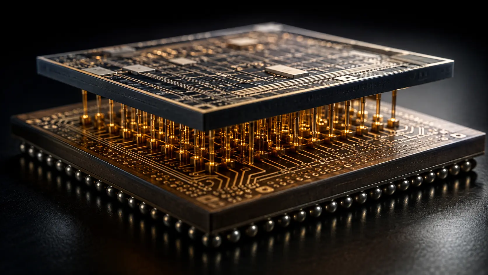

A computer chip is essentially a microscopic city, packed with billions of tiny transistor houses connected by a massive, tangled highway system of metal wires. For decades, engineers built this entire city on a single side of the silicon wafer. Both the power lines bringing electricity in and the data lines moving information around were crammed together in a chaotic, 15-story web hovering above the transistors. But as we shrink transistors down to the atomic scale—approaching the 2-nanometer limit—this city planning has triggered a catastrophic traffic jam. The power wires are now so thin and crowded that they are physically choking the data wires, leaking voltage, and starving the transistors of the energy they need to run complex artificial intelligence calculations.
To prevent Moore’s Law from violently stalling out, the semiconductor industry is executing one of the most radical physical redesigns in computing history: flipping the chip entirely upside down. By carving out a dedicated “basement” exclusively for power delivery, engineers are separating the electricity grid from the data highways. Understanding how foundries are microscopically slicing silicon to route power from the backside is the absolute key to unlocking the next decade of ultra-dense AI supercomputing.
What is Backside Power Delivery Networks (BSPDN)?
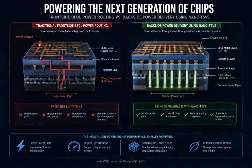
Backside Power Delivery Networks (BSPDN) are an advanced semiconductor manufacturing architecture that relocates the power delivery wires from the top of the silicon wafer to the bottom. By physically separating power routing from signal routing, BSPDN reduces voltage loss, frees up microscopic routing space, and enables significantly denser, faster microchips.
At a Glance
- Concept: Moving the thick electrical power wires to the back of the silicon chip, leaving the top layer strictly for routing data signals.
- Why it matters: In modern chips, power wires take up 20% to 30% of the routing space. Removing them from the top instantly clears massive bottlenecks, allowing for smaller, faster, and more power-efficient sub-2nm transistors.
- Who uses it: Intel (PowerVia), TSMC (A16 Super Power Rail), and Samsung Foundry. It is the defining technology leap required for 2025/2026 AI processors and advanced mobile SOCs.
- Biggest takeaway: Creating BSPDN requires terrifying mechanical precision. Foundries must grind away the bottom of the silicon wafer until it is barely hundreds of nanometers thick, then drill microscopic holes (nano-TSVs) precisely into the back of billions of individual transistors without breaking them.
In Simple Words
Imagine building a skyscraper. For the last 50 years, computer chips have been built like a building where the plumbing (power) and the hallways (data) are shoved into the exact same ceiling space on every floor.
As the building gets taller and the rooms get smaller, that ceiling gets impossibly crowded. The pipes get thinner and longer, which means water pressure drops by the time it reaches the top floor. In a microchip, this is called “IR Drop”—the electricity loses voltage as it fights through tiny, crowded wires, starving the transistors.
Backside Power Delivery solves this by putting all the plumbing in the basement.
Engineers separate the two systems. They keep the data hallways on the top of the chip, but they route all the electrical power directly through the floor from the bottom. Because the power wires have their own dedicated space, they can be made thicker (which means no lost voltage). Because the power wires are gone from the top, there is vastly more room for data wires. The result is a chip that runs cooler, processes data faster, and crams more transistors into a smaller space.
Why This Matters
The semiconductor industry is fighting the physical limits of the universe. Transistors (the switches that compute data) have shrunk to the point where they are measured in individual atoms. We can successfully make a 2-nanometer transistor, but that transistor is entirely useless if we cannot physically run a wire to it.
For data center architects and hardware investors, BSPDN is the primary hardware differentiator of the mid-2020s. Before BSPDN, chips were losing up to 10% of their performance simply because voltage was degrading inside the chip’s internal wiring (the Back-End-of-Line, or BEOL). By migrating to backside power, chipmakers recapture that lost efficiency. A chip featuring BSPDN can operate at higher clock speeds while drawing less power, drastically improving the Performance-per-Watt metric that dictates the total cost of ownership (TCO) for hyperscale AI data centers.
The Foundry War: Intel PowerVia vs TSMC A16
The integration of BSPDN is a tectonic shift in foundry dominance.
For the past five years, TSMC held an undisputed monopoly on bleeding-edge manufacturing with its extreme ultraviolet (EUV) lithography and FinFET scaling. However, Intel aggressively bet its entire turnaround strategy on being the first to mass-produce BSPDN (branded as “PowerVia”) with its Intel 20A and 18A nodes.
This forced TSMC to rapidly accelerate its own BSPDN roadmap, integrating it into the upcoming A16 node. The competition is no longer just about who can draw the smallest transistor gate; it is about who can manipulate the physical silicon substrate to route power most efficiently. This battle has forced equipment manufacturers (like Applied Materials and ASML) to develop entirely new suites of wafer-thinning and bonding tools, spawning a multi-billion-dollar sub-industry within the semiconductor supply chain.
How Backside Power Delivery Networks Work
Completely redesigning the vertical stack of a microchip requires mastering extreme materials science and nanoscale mechanics. Here is the first-principles breakdown.
1. The Fundamental Problem: IR Drop in the BEOL
The wiring above the transistors is called the Back-End-of-Line (BEOL). As transistors shrink, the BEOL wires must also shrink. However, physics dictates that as a wire gets thinner, its electrical resistance increases. When you push electricity through highly resistive, microscopic copper wires, you lose voltage. This is Ohm’s Law ($V = IR$). This “IR Drop” means that a transistor expecting 1.0 volt might only receive 0.85 volts, causing computation errors or forcing the chip to run slower.
2. The Insufficiency of Frontside Routing
Historically, engineers tried to fix this by making the top-level power wires thicker. But power wires compete for the same physical real estate as data signal wires. The more space you dedicate to power, the less space you have to route data logic. Engineers eventually hit a wall: they literally could not fit any more wires on the top of the chip without causing signal interference or manufacturing failures.
3. The Core Mechanism: Flipping the Wafer
To solve this, foundries use Backside Power Delivery. The chip is manufactured normally on the front side (creating the transistors and the data wires). Then, a “carrier wafer” is permanently bonded to the top of the chip to hold it steady. The entire assembly is physically flipped upside down.
4. Technical Depth: Wafer Thinning and nTSV
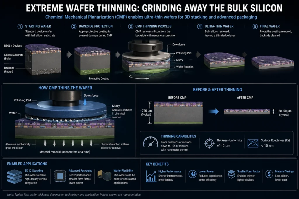
Once flipped, the foundry uses Chemical Mechanical Planarization (CMP) to grind away the thick, inactive silicon substrate on the back of the chip. They shave the wafer from roughly 600 micrometers down to a few hundred nanometers—stopping mere atoms away from the active transistors. Finally, they drill microscopic holes called nano-Through Silicon Vias (nTSV) directly into the back of the transistor’s source/drain contacts. They fill these holes with metal, creating a direct, low-resistance power plug from the basement straight into the transistor.
5. Real-World Consequences: Super Power Rails and Density
Because the power is now entering from the back, the frontside BEOL is completely liberated. Foundries can pack data wires significantly tighter, reducing the size of standard logic cells. In advanced architectures like TSMC’s A16 “Super Power Rail,” the nTSV connects directly to the transistor’s source/drain without using an intermediate buried power rail, achieving maximum atomic density. This architectural leap single-handedly pushes Moore’s Law forward, enabling the sub-2nm era of computing.
BSPDN in Sub-2nm Chips and AI Accelerators
The transition to BSPDN is actively reshaping the roadmaps of the world’s largest fabless chip designers.
NVIDIA and Next-Gen AI Accelerators: Training massive Large Language Models (LLMs) requires GPUs that draw astronomical amounts of power (often exceeding 1,000 watts per chip). Funneling 1,000 watts through microscopic frontside wires creates brutal IR drop. By utilizing BSPDN on upcoming TSMC and Intel foundry nodes, AI chip designers can funnel thick, low-resistance power grids directly into the backside of the GPU cores, unlocking higher clock speeds and significantly improving the energy efficiency of hyperscale training clusters.
Intel’s Clearwater Forest: Intel is utilizing its PowerVia (BSPDN) technology combined with RibbonFET (Gate-All-Around transistors) on its 18A node to produce “Clearwater Forest,” a next-generation Xeon processor designed for cloud data centers. By implementing BSPDN, Intel proved in early test vehicles that they could achieve greater than 90% cell utilization, drastically shrinking the physical size of the die while simultaneously boosting frequency by 6 percent over legacy frontside routing.
Advanced Mobile SOCs (Apple / Qualcomm): Smartphone chips are desperately constrained by physical space and battery life. BSPDN allows companies like Apple to significantly shrink the logic area of their A-series and M-series silicon. A smaller die means shorter data paths, which translates to lower capacitance, less battery drain, and higher performance in the strict thermal limits of a mobile phone chassis.
Economic & Strategic Impact
The adoption of Backside Power Delivery forces a massive Capital Expenditure (CapEx) cycle for semiconductor foundries.
Implementing BSPDN requires inserting brand new, highly complex steps into the middle of the wafer fabrication process. Foundries must invest heavily in advanced wafer-to-wafer bonding equipment to attach the carrier wafer, and extreme metrology tools to ensure that when they drill the nTSVs from the back, they hit a target on the front that is only a few nanometers wide. A misalignment of 10 nanometers completely ruins a $20,000 wafer.
This massive CapEx burden acts as an insurmountable moat. Only the “Big Three” foundries—TSMC, Intel, and Samsung—have the financial scale (spending upwards of $25B-$30B a year) to develop and deploy this technology. Any semiconductor company or nation relying on legacy 2D frontside nodes will be permanently locked out of the ultra-high-performance AI and mobile markets, cementing global reliance on these three fabrication giants.
Advantages
- Eliminates IR Drop: By giving power lines their own dedicated space, the wires can be built thicker and less resistive, ensuring transistors receive perfect, stable voltage.
- Massive Routing Relief: Removing power wires from the frontside frees up 20% to 30% of the routing tracks, solving the signal congestion that plagues traditional multi-layer chips.
- Smaller Die Sizes (Area Scaling): Because the signal wires can be packed much closer together without power wires in the way, the total physical size of the logic blocks can shrink by 10% to 15%, improving wafer yield economics.
- Decoupling Capacitors: Foundries can place massive Metal-Insulator-Metal (MIM) decoupling capacitors directly on the backside of the wafer, right next to the transistors, drastically improving power stability during intense computational bursts.
Limitations
- Extreme Thermal Bottlenecks: Historically, the thick silicon substrate on the back of a chip acted as an excellent heat sink. In BSPDN, that silicon is ground away and replaced with power wires and insulators. Extracting the massive heat generated by the transistors through the backside power network is the most severe physical challenge of the architecture.
- Testing and Debugging Nightmare: If a traditional chip fails, engineers can use microscopes and probes to inspect the top layers. With BSPDN, the chip is sandwiched between complex metal layers on both sides, making it incredibly difficult to physically probe, diagnose, and fix manufacturing defects.
- Mechanical Fragility: Grinding a 300mm silicon wafer down to a few hundred nanometers introduces massive mechanical stress. The wafer becomes highly susceptible to warping, cracking, or delaminating during the extreme heat and pressure of subsequent manufacturing steps.
Common Misconceptions
Misconception: BSPDN makes the transistors themselves smaller.
Reality: BSPDN does not change the size of the actual transistor gate (like transitioning from FinFET to Gate-All-Around). It changes how the transistor is wired. By improving the wiring, you can pack the transistors closer together, but the transistor itself is not shrinking because of BSPDN.
Misconception: Backside power means the chip plugs into the motherboard upside down.
Reality: The entire chip is flipped during the manufacturing process, but to the consumer or the motherboard, the final packaged chip looks completely normal. The complex front/back orientation is handled entirely inside the black epoxy package of the processor.
Misconception: Only Intel is doing this.
Reality: Intel heavily branded their version (“PowerVia”) and aggressive timeline, but it is an industry-wide transition. IMEC (the global semiconductor research hub) pioneered the research, and TSMC, Samsung, and Rapidus all have dedicated backside power architectures entering mass production between 2025 and 2027.
What Most People Miss
The interplay between BSPDN and Gate-All-Around (GAA) Transistors.
BSPDN is rarely deployed alone. It is arriving at the exact same time as the industry transitions away from FinFET transistors to Gate-All-Around (GAA / Nanosheet) transistors.
What most people miss is how perfectly symbiotic these two technologies are. GAA transistors are capable of passing vastly more current than FinFETs, making them incredibly fast, but they are incredibly “hungry.” If you build a GAA transistor using traditional frontside power routing, the thin top wires literally cannot feed the GAA transistor fast enough to reach its true performance potential. BSPDN acts as the high-pressure fuel line required to unlock the true speed of GAA nanosheets. Without backside power, the transition to sub-2nm GAA transistors is mathematically pointless.
Comparison Table
| Feature | Frontside Power Delivery (Legacy) | Backside Power Delivery (BSPDN) |
| Power Routing Location | Top of wafer (BEOL) | Bottom of wafer (Backside) |
| Signal Routing Space | Congested (Shares space with power) | Fully cleared (100% signal data) |
| Voltage Loss (IR Drop) | High (Thin, resistive wires) | Very Low (Thick, dedicated wires) |
| Logic Cell Area | Stagnant (Bound by wire spacing) | Shrinks 10% – 15% |
| Manufacturing Complexity | Standard 2D lithography | Extreme (Wafer bonding, Nano-TSVs) |
| Thermal Dissipation | Heat flows out through bare back | Complex (Back is covered in metal) |
Case Study
Situation: As Intel prepared its foundry roadmap to reclaim the technological crown by 2025, they realized that simply shrinking the transistor was yielding diminishing returns. The performance bottleneck was entirely trapped in the interconnects (the wiring).
Challenge: Implementing Backside Power Delivery and a new transistor architecture (RibbonFET) at the exact same time on a brand-new node (Intel 20A) was deemed incredibly risky. If a chip failed on the line, engineers wouldn’t know if the new transistor failed, or if the new backside wiring failed.
Solution (The Blue Sky Creek Test Vehicle): To de-risk the technology, Intel made a brilliant engineering decision. They decoupled the two breakthroughs. They built an experimental test chip called “Blue Sky Creek.” They used their older, highly reliable, proven transistor technology (Intel Core cores), but they wired it using the brand new PowerVia backside delivery system.
Outcome: The results validated the entire architecture. Because the transistors were a known variable, engineers could isolate the impact of PowerVia. The test chip booted successfully, demonstrated greater than 90% cell utilization, and operated at a 6% higher frequency simply because the IR drop was eliminated.
Lessons Learned: The Blue Sky Creek case study proved to the industry that BSPDN was not just a theoretical lab experiment; it was a manufacturable reality. By proving they could successfully flip a wafer, grind it down, and route power from the back without shattering the silicon, Intel validated the roadmap for the entire sub-2nm generation, forcing TSMC and Samsung to aggressively match their timeline.
Future Outlook
Next 12–24 Months
The era of Volume Production and Yield Wars. Between late 2024 and 2026, Intel 20A/18A and TSMC A16 will ramp into high-volume manufacturing (HVM). The immediate focus will be purely on yield—how many chips on a 300mm wafer actually survive the extreme mechanical grinding and nTSV drilling without defecting. The foundry that masters the defect density of the wafer-bonding process will dominate the early contracts for 2026 AI accelerators and premium smartphone SOCs.
Next 3–5 Years
The evolution of Direct Source-to-Drain Routing. Early iterations of BSPDN use a “Buried Power Rail” (BPR), where the backside via connects to a small rail buried under the transistor. By 2027/2028, architectures like TSMC’s “Super Power Rail” will mature, completely bypassing the buried rail and drilling the backside contact directly into the transistor’s source and drain. This atomic-level precision represents the absolute maximum limit of 2D density, pushing standard logic cells to their smallest physical geometries.
Next 10 Years
The transition to 3D Heterogeneous Power Routing. As the industry fully commits to 3D packaging (stacking multiple chiplets on top of each other), backside power networks will become the foundational highway of the 3D stack. The backside of one logic chip will serve as the power grid for the memory chip stacked directly underneath it. By the 2030s, BSPDN will enable monolithic 3D ICs where power, logic, and memory are woven together in a seamless, three-dimensional silicon cube, marking the final stage of Moore’s Law scaling.
Most Likely Scenario
BSPDN will become the mandatory, ubiquitous standard for all high-performance silicon. Just as the industry fully abandoned planar transistors for FinFETs a decade ago, frontside power delivery will be completely abandoned for AI, HPC, and mobile architectures. The massive CapEx required to execute it will solidify TSMC, Intel, and Samsung as the only three entities on Earth capable of fabricating the digital infrastructure of the late 2020s.
Key Takeaways
- Backside Power Delivery Networks (BSPDN) completely redesign microchips by moving all electrical power lines from the top of the chip to the bottom.
- Traditionally, power and data wires compete for space on the top of the chip, creating a severe bottleneck and causing electricity to lose voltage (“IR Drop”) through tiny, crowded wires.
- By moving power to the back, foundries can make power wires thicker (eliminating IR Drop) and free up 20% to 30% of the frontside space exclusively for routing data signals.
- Manufacturing BSPDN requires extreme precision: the silicon wafer is flipped, ground down to a few hundred nanometers, and pierced with microscopic vias (nano-TSVs) to plug power directly into the transistors.
- Intel (PowerVia) and TSMC (A16 Super Power Rail) are aggressively deploying this architecture for 2025/2026 production, making it the defining technology of the sub-2nm era.
- The primary challenge moving forward is thermal management, as the thick silicon substrate that historically acted as a heat sink is ground away and replaced by complex metal wiring.
Glossary
Back-End-of-Line (BEOL): The second major portion of semiconductor fabrication where individual devices (transistors) get interconnected with wiring on the top of the wafer.
Chemical Mechanical Planarization (CMP): A highly precise polishing process that uses chemical slurries and mechanical grinding to shave away microscopic layers of silicon and metal to perfectly flatten a wafer.
FinFET / Gate-All-Around (GAA): Architectures of transistors. FinFETs use a 3D fin for the gate. GAA completely surrounds the channel for better electrical control. BSPDN is highly synergistic with GAA.
IR Drop: Voltage drop across a conducting path ($V = I \times R$). In chips, it refers to the loss of electrical pressure as power struggles to get through extremely thin, resistive copper wires.
nano-Through Silicon Via (nTSV): A microscopic vertical electrical connection (hole) passing completely through a silicon wafer, used to connect the backside power grid to the frontside transistors.
Wafer Thinning: The mechanical process of grinding away the thick, inactive bottom layer of a silicon wafer to expose the backside of the transistors.
Frequently Asked Questions
Why did it take so long to put power on the back of the chip?
It wasn’t a physics problem; it was an engineering and mechanical problem. Grinding a silicon wafer down to the thickness of a few hundred nanometers makes it incredibly fragile. It took decades to invent the wafer-bonding equipment and precision lasers necessary to handle the silicon without shattering it.
Does this make the microchip physically thicker?
No, it actually makes the active part of the chip denser. While you are adding metal to the back, you are grinding away the massive, unused bulk silicon substrate that used to sit there. The overall physical thickness of the packaged chip remains virtually identical.
Will this make my phone battery last longer?
Yes. Because BSPDN eliminates IR Drop, the chip’s internal power delivery is vastly more efficient. The processor wastes less energy fighting wire resistance, which translates directly to longer battery life and cooler temperatures in the exact same physical chassis.
What is the difference between TSMC’s Super Power Rail and Intel’s PowerVia?
They are fundamentally the same concept (BSPDN), but they differ in microscopic execution. Intel’s early iterations utilize a “buried power rail” where the via connects to a tiny metal bar under the transistor. TSMC’s A16 “Super Power Rail” aims to bypass the buried rail entirely, connecting the via directly into the atomic source/drain of the transistor for absolute maximum density.
Can legacy chip factories be upgraded to do this?
Not easily. BSPDN requires an entirely new suite of fabrication tools placed in the middle of the cleanroom workflow. Foundries cannot just flip a switch; they have to spend billions of dollars installing new CMP grinders, wafer bonders, and advanced lithography alignment tools, which is why only the absolute largest foundries can afford the transition.
Sources
[1] imec: The road to Backside Power Delivery: from concepts to manufacturing (Research Briefs 2025)
[2] TSMC: A16 Technology Node and Super Power Rail Architecture Overview (Symposium Data 2025)
[3] Intel Corporation: PowerVia: Intel’s Backside Power Delivery Network (Technology Showcase)
[4] IEEE Spectrum: How Flipping the Chip Upside Down Will Save Moore’s Law
[5] Semiconductor Engineering: Thermal Challenges and Metrology for Backside Power Delivery