Advertisement
)
AT A GLANCE
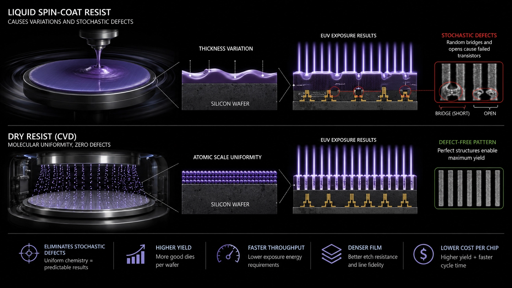
- Concept: Liquid Spin-Coating: Legacy manufacturing relies on physically spinning liquid chemicals over a wafer, causing microscopic inconsistencies.
- Concept: Chemical Vapor Deposition: Dry resist turns chemicals into a gas, settling perfectly uniform molecular layers onto the silicon.
- Concept: Stochastic Defects: Random variations in chemical thickness cause the extreme ultraviolet light to misprint microscopic transistors.
- Concept: Yield Economics: Perfecting chemical uniformity directly increases the percentage of usable, sellable artificial intelligence chips per wafer.
HOW IT WORKS
Printing a semiconductor requires a light-sensitive chemical called a photoresist. When ultraviolet light hits this chemical, it hardens or dissolves, creating a physical stencil on the silicon wafer.
For the past fifty years, the industry applied this resist by dispensing a puddle of liquid chemical onto the center of a silicon wafer and spinning it at thousands of revolutions per minute. The centrifugal force spreads the liquid outward into a thin film.
This mechanical spinning reaches its physical limit at the two-nanometer node. When dealing with extreme ultraviolet (EUV) light, the liquid resist creates microscopic variations in thickness, sometimes clustering chemical molecules unevenly across the wafer edge.
When an EUV photon strikes an uneven cluster, it causes a stochastic defect. The light fails to expose the resist correctly, leaving random, microscopic bridges of unhardened chemical that physically short-circuit the printed transistor.
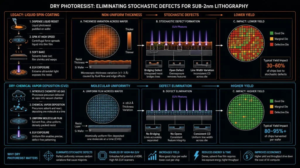
To solve this, hardware manufacturers like Lam Research developed dry photoresist technology. Instead of spinning a liquid, engineers place the silicon wafer inside a sealed vacuum chamber. They introduce the photoresist chemistry as a highly controlled gaseous vapor.
Through Chemical Vapor Deposition (CVD), this gas settles onto the wafer exactly one molecule at a time. This process builds a pristine, ultra-dense chemical stack that is perfectly uniform across the entire 300-millimeter silicon surface, completely eliminating the centrifugal inconsistencies of liquid spin-coating.
WHY IT MATTERS NOW
The semiconductor industry is attempting to scale down to the angstrom era, building transistors narrower than a strand of human DNA. At this microscopic scale, a single misplaced photon or a slightly thick puddle of liquid chemical ruins the entire multi-thousand-dollar processor.
Advanced foundries like TSMC and Intel are deploying ASML’s High-NA (Numerical Aperture) EUV scanners. These massive, $350 million machines focus light with unprecedented sharpness, but their extreme precision is entirely wasted if the underlying photoresist chemical is physically uneven.
Dry photoresist acts as the mandatory chemical bridge that allows High-NA lithography to actually function. By eliminating stochastic defects, the vapor deposition process drastically increases the yield rate—the total percentage of fully functional, sellable chips harvested from a single silicon wafer.
This yield rate dictates the global unit economics of artificial intelligence. If a foundry can only harvest forty percent of the chips on a wafer due to chemical blurring, they must charge astronomical prices to break even. Doubling that yield through dry resist deposition physically lowers the baseline manufacturing cost of the hardware required to train next-generation neural networks.
WHAT MOST PEOPLE MISS
Industry observers obsess over the sheer size and cost of the ASML lithography machines, assuming the laser optics alone dictate Moore’s Law. They completely miss the reality that semiconductor scaling is currently bottlenecked by organic chemistry, not optical physics.
Because liquid resist must remain stable in a bottle during shipping, chemical suppliers pump it full of heavy solvent fluids. When the liquid spins onto the wafer, these solvents must bake out, causing the chemical film to shrink and warp unpredictably. Dry resist eliminates the solvent entirely. By depositing the chemical purely as a gas, engineers construct a tighter, more dense molecular matrix. This dense matrix requires less total light energy to properly expose, allowing foundries to run their massive EUV scanners faster, directly increasing the total hourly output of the fabrication plant.
THE TRAJECTORY
Next 12–36 Months: Top-tier logic foundries will implement dry resist chemical vapor deposition exclusively for the most critical, hyper-dense metal routing layers on sub-2nm nodes, maintaining cheaper liquid resist for less complex chip sections.
Next Five Years: Equipment manufacturers will integrate the dry resist deposition chamber and the EUV exposure scanner into a single, contiguous high-vacuum track. This integration will prevent ambient cleanroom air from ever touching the highly sensitive chemical film, further driving down defect rates.
Next Ten Years: Dry photoresist architectures will scale to support pattern-directed self-assembly. Gaseous chemical layers will be engineered to spontaneously arrange themselves into perfect nanometer structures when exposed to light, completely bypassing the need for physical optical stencils.
What Could Go Wrong: The chemical precursors required for dry vapor deposition are highly toxic and violently reactive when exposed to oxygen. A single microscopic leak in the vacuum supply lines would instantly trigger a severe chemical fire, shutting down the entire multi-billion-dollar fabrication floor for weeks of decontamination.
Most Likely Outcome: Dry photoresist will entirely replace liquid spin-coating for all advanced logic and memory nodes. The capability to deposit pristine chemical films at the single-molecule level will become the defining differentiator between elite foundries capable of angstrom-level scaling and those permanently stuck at legacy geometries.
KEY TERMS
- Photoresist: A light-sensitive chemical applied to a silicon wafer that hardens or dissolves when exposed to ultraviolet light, acting as a microscopic stencil.
- Spin-Coating: A legacy manufacturing technique that applies liquid chemicals to a wafer by spinning it at high speeds to spread the fluid outward.
- Chemical Vapor Deposition (CVD): A vacuum process that introduces chemical precursors as a gas to deposit perfectly uniform, molecule-thick solid layers onto a substrate.
- Stochastic Defect: A random, unpredictable manufacturing failure caused by microscopic variations in chemical thickness or photon distribution during extreme ultraviolet lithography.
- Yield Rate: The mathematical percentage of fully functional, sellable microchips successfully harvested from a single processed silicon wafer.
SOURCES
- Lam Research — Dry Resist Technology for High-NA EUV Lithography
- SPIE (International Society for Optics and Photonics) — Stochastic Defect Mitigation in EUV Patterning via Chemical Vapor Deposition
- ASML — High-NA EUV Ecosystem and Photoresist Requirements
- IEEE Transactions on Semiconductor Manufacturing — Yield Economics and Defect Density in Angstrom-Era Nodes