Advertisement
)
AT A GLANCE
- Concept: The Gate Dielectric: A physical barrier that controls whether electrical current flows or stops inside a silicon transistor.
- Concept: Quantum Tunneling: When a physical barrier becomes too thin, subatomic particles can literally pass straight through solid matter.
- Concept: Dielectric Constant (K): A measure of a material’s ability to store electrical energy within an electric field.
- Concept: Hafnium Oxide: Replacing legacy silicon dioxide with this heavier material allows foundries to build physically thicker walls that maintain strong electrical control.
HOW IT WORKS
A computer processor operates through billions of microscopic switches called transistors. Each switch has a “gate” that opens to let current flow (registering a binary 1) or closes to stop it (registering a binary 0).
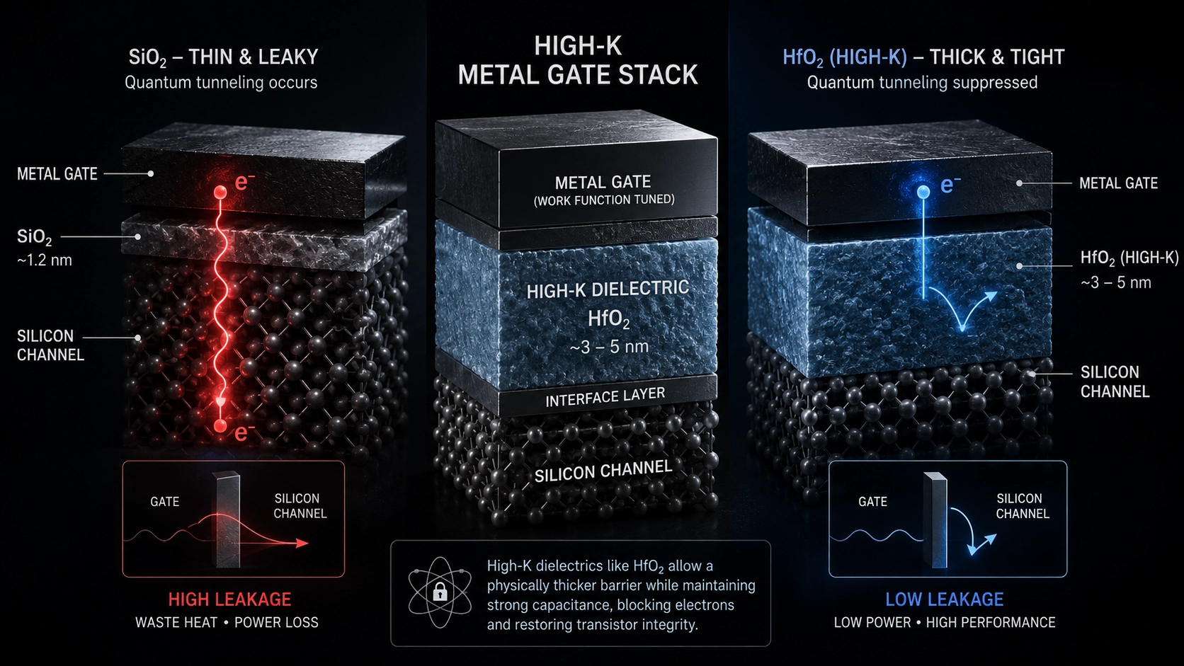
Between this gate and the underlying silicon channel sits a critical insulator known as the gate dielectric. For decades, the semiconductor industry used simple silicon dioxide (SiO₂) for this barrier. As manufacturers aggressively shrank the size of transistors to cram more processing power onto a chip, they were forced to physically thin this SiO₂ layer.
By the 45-nanometer node, this SiO₂ barrier became a mere 1.2 nanometers thick—roughly the width of five individual silicon atoms. At this extreme microscopic scale, classical physics breaks down and quantum mechanics takes over.
When a barrier is only five atoms thick, an electron no longer views it as a solid wall. Through a phenomenon known as quantum tunneling, the electron probabilistically “teleports” from the silicon channel directly through the closed gate. The switch is supposed to be off, but electricity leaks through anyway. This leakage generates massive amounts of waste heat and drains the battery instantly.
To fix this, engineers replace the silicon dioxide with a “High-K” material, specifically hafnium-based compounds. The “K” refers to the dielectric constant (κ).The physical capacitance (C) of the gate is defined by the equatio.
$$C = \frac{\kappa \cdot \varepsilon_0 \cdot A}{t}$$
Where:
- ε₀ is the permittivity of free space.
- A is the gate area.
- t is the physical thickness of the barrier.
Because hafnium oxide has a dielectric constant (κ) roughly five times higher than SiO₂, engineers can make the physical wall (t) significantly thicker. This increase happens without losing the electrical control required to switch the transistor. Ultimately, this thicker wall completely blocks quantum tunneling, restoring the binary integrity of the switch.
WHY IT MATTERS NOW
Quantum tunneling is not a theoretical physics problem; it is the absolute thermodynamic limit capping the global artificial intelligence boom. Without High-K Metal Gate (HKMG) technology, modern sub-5-nanometer computing physically cannot exist.
If TSMC or Intel attempted to build a modern GPU using legacy SiO₂ gates, the chip would draw hundreds of thousands of watts of idle power just sitting on a desk. The quantum leakage would instantly vaporize the silicon the moment the chip was plugged in. HKMG is the specific material science breakthrough that prevents modern hyperscale data centers from spontaneously catching fire.
The integration of HKMG completely altered the economics of global semiconductor manufacturing. Depositing a perfect, uniform layer of hafnium oxide requires advanced atomic layer deposition (ALD) machines, forcing the industry to transition away from simple, high-temperature oxygen baking.
Because hafnium oxide reacts poorly with traditional polysilicon gate electrodes, engineers also had to replace the electrode itself with complex, multi-layered metal alloys—hence the “Metal Gate” in the name. Tuning the specific work function of these new metals requires depositing materials like titanium nitride or tantalum exactly one atomic layer at a time. This extreme material complexity heavily consolidated the industry, leaving only three global foundries capable of mastering the chemistry required to produce advanced logic chips.
WHAT MOST PEOPLE MISS
Tech media enthusiastically reports on the transition from FinFET to Gate-All-Around (GAA) transistor geometries, assuming new physical shapes alone drive performance. They completely miss that these new 3D architectures are highly dependent host structures built exclusively to wrap the High-K dielectric completely around the silicon channel.
The shape of the transistor only matters because it maximizes the surface area of the hafnium oxide barrier. Furthermore, the hafnium itself is highly sensitive to defect states. If a single stray oxygen atom is missing from the deposited hafnium lattice, it creates a microscopic “trap.” Electrons fall into these traps during operation, permanently shifting the voltage required to turn the transistor on. Over time, this atomic degradation causes the entire processor to slowly drift out of specification and fail, dictating the physical lifespan of the hardware powering global cloud infrastructure.
THE TRAJECTORY
Next 12–36 Months: Foundries will transition from hafnium oxide to advanced doped-hafnium and zirconium-based dielectrics. These new chemical matrices will squeeze the final remaining fractions of capacitance out of the gate stack, enabling the immediate transition to 2-nanometer Gate-All-Around architectures.
Next Five Years: Manufacturers will integrate ferroelectric High-K materials directly into the gate stack. These materials possess a natural physical memory; by shifting their atomic polarization, the transistor can retain its 1 or 0 state even when the power is completely disconnected, fundamentally merging logic processing and long-term data storage into a single component.
Next Ten Years: The physical thickness limit of hafnium will be reached. The industry will be forced to transition away from silicon entirely, migrating to Two-Dimensional (2D) transition metal dichalcogenides (TMDs) like molybdenum disulfide. These atom-thick semiconductors will require entirely novel, yet-to-be-discovered dielectric materials to contain the extreme quantum forces at the sub-angstrom level.
What Could Go Wrong: The extreme temperatures required to anneal (bake) the adjacent silicon components can physically crystallize the hafnium oxide layer. If the High-K material crystallizes, it instantly forms “grain boundaries”—microscopic physical cracks in the barrier that act as superhighways for electrical leakage, instantly destroying the chip’s power efficiency.
Most Likely Outcome: High-K Metal Gate stacks will remain the undisputed material foundation for all high-performance computing. However, as the physical geometry shrinks to the absolute limits of the periodic table, the focus will shift entirely from mechanical engineering to exotic, single-atom material chemistry to hold back the laws of quantum mechanics.
KEY TERMS
- High-K Dielectric: A material with a high dielectric constant ($\kappa$) that replaces silicon dioxide in transistors, allowing for a physically thicker barrier without losing electrical capacitance.
- Quantum Tunneling: A quantum mechanical phenomenon where a subatomic particle, like an electron, passes through a physical barrier that classical physics says it should not be able to cross.
- Hafnium Oxide (HfO₂): A dense, heavy-metal oxide compound that is the primary material used to construct modern High-K gate barriers.
- Work Function: The minimum amount of thermodynamic energy required to remove an electron from the surface of a solid metal, a critical metric for tuning the switching voltage of a transistor gate.
- Atomic Layer Deposition (ALD): A precision manufacturing technique used to build materials slowly by depositing chemical gases exactly one single layer of atoms at a time.
SOURCES
- IEEE Electron Device Letters — High-K Gate Dielectrics: Current Status and Materials Properties Considerations
- Intel Corporation — The High-K Metal Gate Revolution and Sub-Node Scaling Mechanics
- Nature Materials — Ferroelectric Hafnium Oxide for Next-Generation Logic and Memory Devices
- TSMC — Advanced Materials Research: Dielectric Scaling in Gate-All-Around Architectures