Advertisement
)

AT A GLANCE
- Concept: The Magnetic Tunnel Junction: Two magnetic metal plates separated by an insulating barrier only atoms thick.
- Concept: Spin Polarization: The system filters electrons so their quantum spins align in a single uniform direction.
- Concept: Angular Momentum Transfer: The aligned electrons physically strike the free magnetic layer, forcing it to flip its orientation.
- Concept: Non-Volatile Speed: The memory retains data without constant power while matching the speed of volatile SRAM.
HOW MRAM WORKS
Standard computer memory stores data by trapping electrons inside a silicon capacitor. Because capacitors leak, the system must constantly supply fresh electricity to maintain the stored information. Magnetoresistive Random Access Memory (MRAM) abandons electrical charge entirely. It stores data using the quantum property of electron spin.
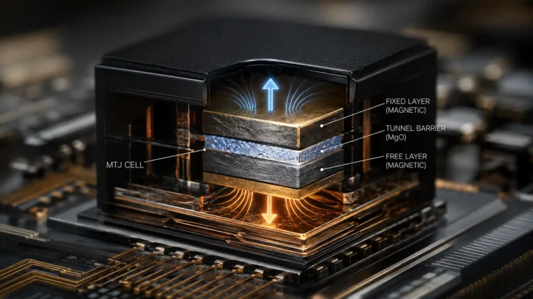
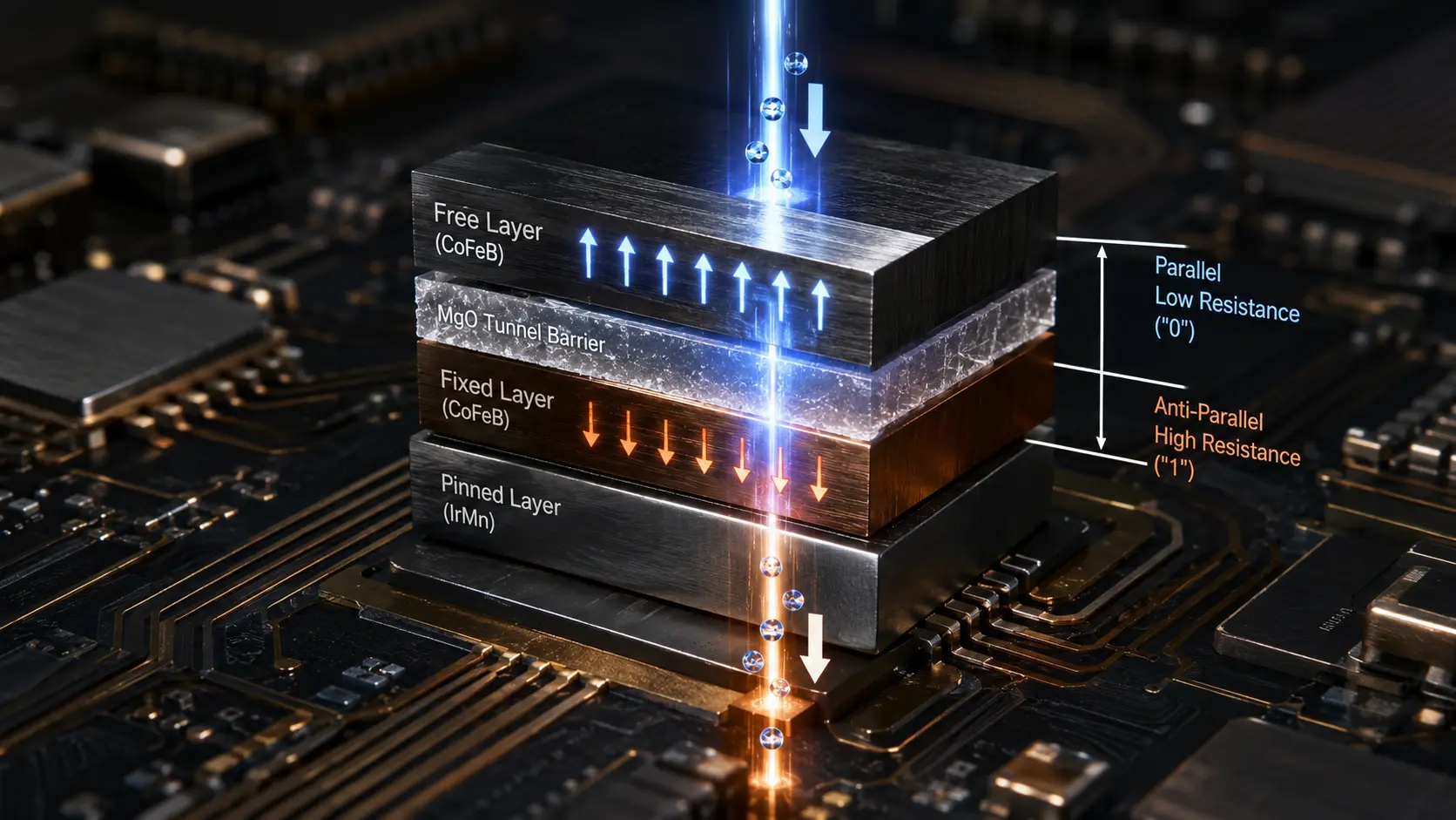
The core component of MRAM is the Magnetic Tunnel Junction (MTJ). An MTJ consists of two ferromagnetic layers separated by a microscopic insulating barrier, typically magnesium oxide (MgO). The manufacturer permanently fixes the magnetic alignment of the bottom layer, while the top layer remains free to switch its magnetic orientation.
To write data, the system relies on Spin-Transfer Torque (STT). A circuit pushes a burst of electrical current through the fixed magnetic layer. This layer acts as a polarizing filter, forcing the quantum spin of the passing electrons to align in a single direction.
These spin-polarized electrons tunnel through the thin MgO barrier and strike the free magnetic layer. The electrons physically transfer their quantum angular momentum to the free layer, forcing its magnetic field to flip. If the two layers align in parallel, electrical resistance drops, creating a binary “0”. If they oppose each other, resistance spikes, creating a binary “1”.
WHY IT MATTERS NOW
The semiconductor industry faces a severe power consumption crisis at the edge of the network. Billions of Internet of Things (IoT) sensors, autonomous vehicles, and industrial robotics require massive amounts of localized memory. Historically, designers used Static RAM (SRAM) for speed and Flash memory for permanent storage.
SRAM consumes up to forty percent of the physical space on a modern processor die and constantly leaks electricity. Flash memory retains data without power, but it writes data too slowly to support real-time algorithmic processing. STT-MRAM perfectly bridges this gap. It matches the read-write speed of SRAM while providing the permanent, zero-leakage storage of Flash.
Global semiconductor foundries, including TSMC and GlobalFoundries, now embed MRAM directly into the logic processors of edge devices. This embedded MRAM (eMRAM) allows microcontrollers to wake from a zero-power sleep state instantly. The chip does not need to waste time and electricity loading an operating system from an external storage drive, because the working memory never forgot the data.
This physical hardiness also dictates the architecture of the modern space economy. Standard silicon memory flips randomly when struck by cosmic radiation, causing satellite computers to crash. Because MRAM stores data magnetically rather than electrically, it is inherently radiation-hardened, making it the mandatory memory architecture for proliferated low earth orbit defense constellations.
WHAT MOST PEOPLE MISS
Technical discussions of MRAM emphasize its infinite endurance compared to the rapid degradation of Flash memory cells. They completely ignore the brutal atomic stress applied to the Magnetic Tunnel Junction during the writing process. Pushing a high-density, spin-polarized current through a magnesium oxide barrier that is only three atoms thick causes severe electromigration.
To flip the magnetic free layer faster, engineers must increase the electrical current. However, this higher current physically fractures the crystalline lattice of the MgO insulator over time. Balancing the write current—providing enough torque to flip the magnet but keeping it low enough to prevent physical barrier destruction—remains the absolute boundary limiting STT-MRAM from replacing high-density server memory in hyperscale data centers.
THE TRAJECTORY
Next 12–36 Months: Major automotive manufacturers will transition advanced driver-assistance systems (ADAS) to microcontrollers utilizing embedded MRAM. This shift ensures self-driving processors retain critical sensor data instantly during sudden power failures, preventing catastrophic memory wipes during accidents.
Next Five Years: The commercial scaling of Spin-Orbit Torque (SOT) MRAM. Engineers will decouple the read and write paths of the memory cell. By routing the heavy write current underneath the cell rather than directly through the fragile magnesium oxide barrier, SOT-MRAM will eliminate physical degradation, unlocking speeds fast enough to finally replace lower-level CPU cache memory.
Next Ten Years: The integration of MRAM into neuromorphic computing grids. Because MRAM cells can simulate the analog weighting and non-volatile states of biological synapses, hardware designers will use magnetic junctions to physically build neural networks in silicon, eliminating the need to move data between logic and memory entirely.
What Could Go Wrong: Extreme thermal sensitivity during chip manufacturing. The magnetic layers inside an MTJ degrade rapidly when exposed to temperatures above 400°C. If logic foundries cannot lower the high heat currently required to bake standard copper interconnects onto the silicon wafer, the manufacturing process itself will melt the embedded magnetic memory, destroying yield rates.
Most Likely Outcome: STT-MRAM will monopolize the embedded memory market for edge computing, IoT, and aerospace. However, due to the physical difficulty of shrinking the magnetic barrier past the 14-nanometer node without triggering quantum tunneling leaks, it will fail to replace cheap, ultra-dense DRAM in the core data center.
KEY TERMS
- Magnetic Tunnel Junction (MTJ): A microscopic component consisting of two magnetic layers and a thin insulator, where electrical resistance changes based on magnetic alignment.
- Spin-Transfer Torque (STT): The quantum mechanical effect where an electrical current alters the magnetic orientation of a material by transferring the angular momentum of its electrons.
- Non-Volatile Memory (NVM): A classification of computer memory that physically retains its stored data even after the primary power source is disconnected.
- Free Layer: The specific magnetic layer within an MTJ whose magnetic field is designed to flip its orientation to record a binary one or zero.
- Electromigration: The gradual, destructive displacement of metal atoms in a semiconductor caused by the momentum transfer of flowing electrons under high current density.
SOURCES
- Institute of Electrical and Electronics Engineers (IEEE) — Spin-Transfer Torque MRAM: Technology and Foundry Integration
- TSMC (Taiwan Semiconductor Manufacturing Company) — Embedded MRAM Architecture for Advanced Logic Nodes
- Defense Advanced Research Projects Agency (DARPA) — Non-Volatile Logic and Radiation-Hardened Magnetic Memory Systems
- Journal of Applied Physics — Degradation Mechanisms and Dielectric Breakdown in MgO-based Magnetic Tunnel Junctions