Advertisement
)
AT A GLANCE
- Concept: Nano-Abrasives: Suspended silica or ceria particles physically scrape away excess material from the wafer surface.
- Concept: Chemical Etching: Proprietary oxidizers dissolve specific metals or dielectrics without damaging adjacent components.
- Concept: Planarization: Flattening each individual layer allows lithography machines to maintain perfect optical focus.
- Concept: Defect Tolerance: A single microscopic scratch ruins the entire die, making slurry purity an absolute necessity.
HOW IT WORKS
Modern semiconductor fabrication is a rigorous process of stacking vertical layers of transistors and copper interconnects. After depositing a new layer of metal or insulating material, the surface of the silicon wafer becomes extremely uneven. You cannot print the next layer onto a bumpy surface because the depth of focus for extreme ultraviolet lithography is incredibly shallow.
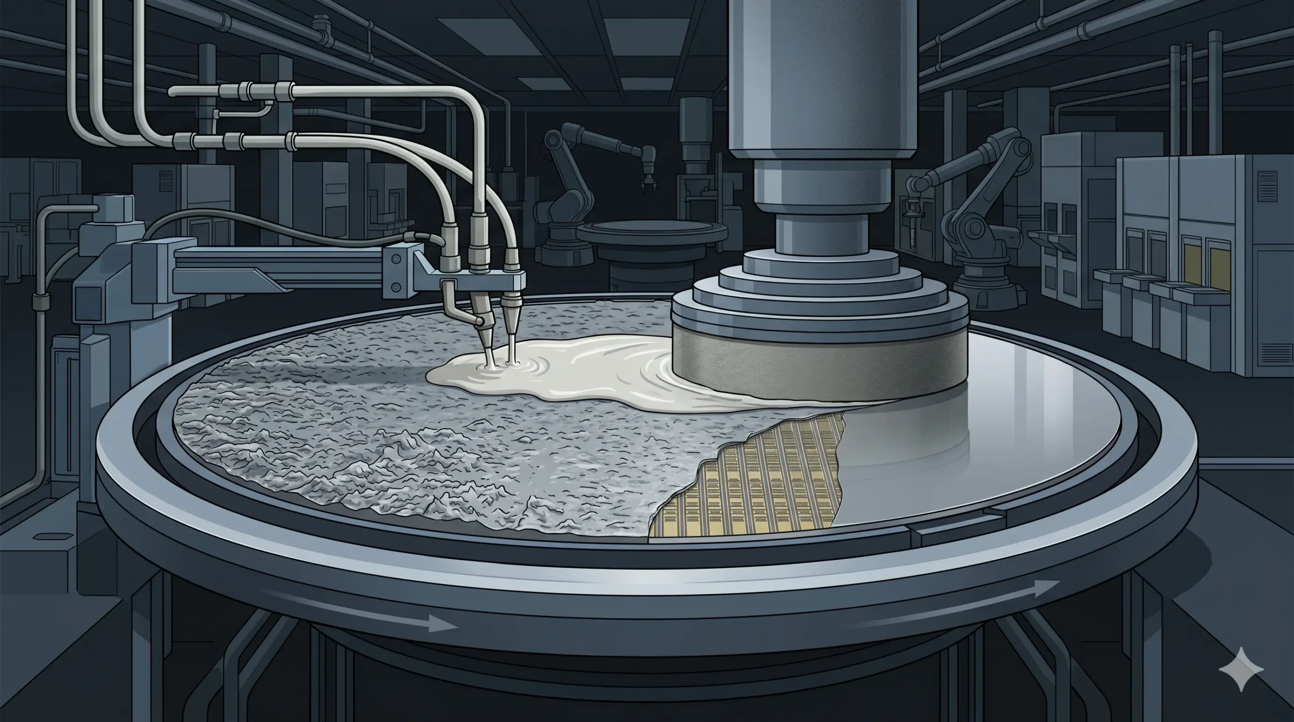
To restore a perfectly flat surface, manufacturing tools press the rotating wafer face-down onto a polyurethane polishing pad. The system continuously dispenses chemical mechanical planarization (CMP) slurry between the pad and the wafer. This fluid acts simultaneously as a chemical solvent and a physical sandpaper.
The slurry contains highly controlled oxidizers, such as hydrogen peroxide, and microscopic abrasive particles like colloidal silica or ceria. The chemicals react with the solid material on the wafer—such as excess copper or tungsten—turning the top atomic layer into a softer oxidized film.
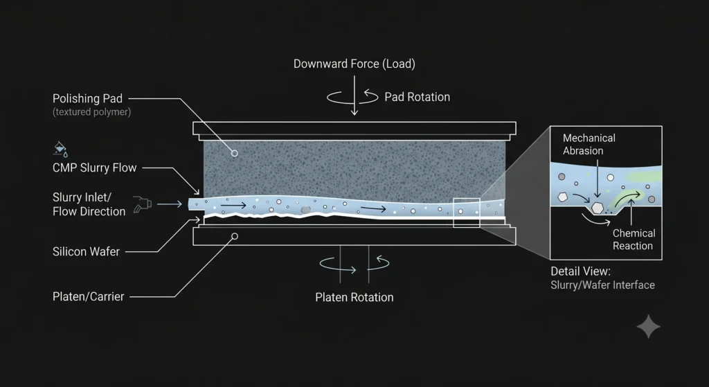
The abrasive particles then mechanically sweep away this softened film as the wafer rotates against the pad. The material removal rate ($MRR$) generally follows Preston’s Equation:
$$MRR = K_p \times P \times V$$
Where $K_p$ is Preston’s coefficient accounting for specific slurry chemistry and pad material, $P$ represents the downward mechanical pressure applied to the wafer, and $V$ is the relative sliding velocity between the wafer and the pad.
Engineers formulate specific slurries to halt the polishing process automatically. By adding precise polymer surfactants, the slurry coats and protects certain materials while aggressively dissolving others, achieving the exact planarization depth required for advanced 3-nanometer logic nodes.
WHY IT MATTERS NOW
Advanced computing relies on dense vertical integration. As foundries transition to 3-nanometer nodes and backside power delivery networks, the number of stacked layers on a single silicon die frequently exceeds eighty. Every single layer requires a flawless CMP step before the next sequence can begin.
A single multi-million-dollar wafer contains hundreds of high-performance logic chips. If the slurry introduces a micro-scratch or leaves a nanometer of uneven material, the electrical interconnects fail to align. This defect ruins the entire vertical stack, directly destroying the fab’s yield and erasing millions in invested capital.
Geopolitics increasingly restrict access to the rare earth materials used in these precise abrasives. High-efficiency ceria nanoparticles, required to polish advanced insulating dielectrics quickly, originate almost entirely from tightly controlled mining operations in China. Finding synthetic alternatives dictates the strategic timeline for next-generation Western foundries.
Equipment giants like Applied Materials manufacture the massive polishing tools, but specialty chemical companies command the recurring revenue. Suppliers who master the extreme fluid dynamics and polymer chemistry of node-compliant slurries capture a highly defensible monopoly over the physical baseline of global compute.
Foundry operators closely guard their specific slurry recipes. Industry leaders view these fluid compositions as primary intellectual property, knowing that superior planarization physics allows them to stack more layers than their rivals without inducing structural failures.
WHAT MOST PEOPLE MISS
Mainstream technology analysis focuses obsessively on the photolithography machines that print the transistor patterns. Observers treat silicon fabrication purely as an optical challenge, assuming that better lasers automatically yield better chips.
They completely ignore the physical tribology that makes lithography possible. Extreme ultraviolet light cannot focus on a warped, microscopic mountain range of copper and silicon dioxide. The CMP slurry serves as the strict physical reset button for the wafer.
The fluid dynamics of the slurry distribution directly dictate the defect rate. If the slurry aggregates into slightly larger particle clusters during transit, these clusters act like microscopic boulders on the polishing pad. This physical aggregation gouges deep trenches into the silicon, destroying billions of interconnects instantly and proving that chemical stability dictates manufacturing yield.
THE TRAJECTORY
Next 12–36 Months: Fabs will transition to ultra-selective slurries containing self-stopping polymers that prevent over-polishing during complex 3D packaging sequences.
Next Five Years: Closed-loop artificial intelligence systems will dynamically adjust slurry flow rates and pressure variables in real-time. These systems will rely on optical sensors to detect planarization depth down to the angstrom across the rotating pad.
Next Ten Years: The physical limits of mechanical pressure will force the industry to adopt purely chemical, contact-free planarization methods. Sub-nanometer transistor gates will become too fragile to survive physical abrasion, requiring purely solvent-based topography leveling.
What Could Go Wrong: Contamination within the slurry supply chain poses a systemic risk. A single miscalibrated batch of abrasive nanoparticles will scratch and ruin thousands of wafers before quality control systems detect the anomaly, halting entire production lines.
Most Likely Outcome: CMP slurries will become highly customized, proprietary formulations engineered specifically for individual chip designs. This extreme specialization will tie foundry success directly to localized, highly secure chemical supply chains.
KEY TERMS
- Chemical Mechanical Planarization (CMP): The process of smoothing surfaces with the combination of chemical and mechanical forces to flatten a silicon wafer.
- Preston’s Equation: A mathematical formula used to predict the material removal rate during polishing based on applied pressure and velocity.
- Slurry: A semi-liquid mixture consisting of microscopic abrasive particles suspended in a highly engineered chemical solvent.
- Tribology: The science of interacting surfaces in relative motion, encompassing the principles of friction, lubrication, and physical wear.
- Depth of Focus: The specific vertical distance over which a lithography machine can maintain sharp optical resolution on a target surface.
SOURCES
- Applied Materials — CMP Technology and Advanced Node Planarization
- IEEE Transactions on Semiconductor Manufacturing — Modeling Material Removal Rates in Chemical Mechanical Planarization
- TSMC — Advanced Wafer Level Packaging and Topography Management
- Journal of The Electrochemical Society — Tribological Attributes of CMP Processes