Advertisement
)
AT A GLANCE
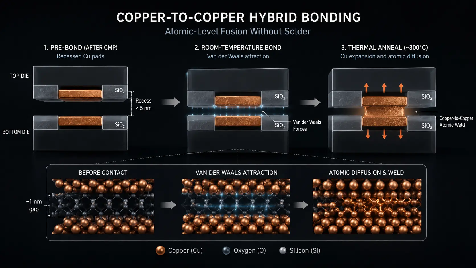
- Concept: Solderless Fusion: Silicon dies bond atomically without traditional melting metals or physical adhesives.
- Concept: Van der Waals Forces: Extreme surface smoothness allows molecular attraction to pull the chips together naturally.
- Concept: Chemical Mechanical Planarization: Abrasive polishing creates ultra-flat surfaces with copper pads slightly recessed below the oxide.
- Concept: Thermal Annealing: Applied heat forces the copper atoms to expand, collide, and permanently weld together.
HOW IT WORKS
Traditional semiconductor packaging connects chips using microscopic spheres of solder known as micro-bumps. As engineers pack more transistors into artificial intelligence accelerators, these solder bumps become a physical bottleneck. If placed too closely together, the melting solder bridges the gap between adjacent pads, causing an immediate electrical short circuit.
Hybrid bonding eliminates the solder entirely by directly fusing the copper wiring of two separate silicon dies. The process begins with chemical-mechanical planarization (CMP). Precision polishing equipment grinds the surface of both chips until they achieve extreme nanometer-level flatness.
The CMP process uses specific chemical slurries to polish the copper slightly faster than the surrounding silicon dioxide dielectric. This dynamic creates a microscopic recess—often less than five nanometers deep—where the copper pad sits just below the glass-like oxide surface.
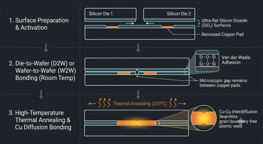
When automated robotic bonders align and press the two chips together at room temperature, the ultra-flat silicon dioxide surfaces immediately fuse. This initial adhesion relies entirely on van der Waals forces, mathematically described by the Lennard-Jones potential:
$$V(r) = 4\epsilon \left[ \left(\frac{\sigma}{r}\right)^{12} – \left(\frac{\sigma}{r}\right)^6 \right]$$
Where V(r) is the intermolecular potential, ε (epsilon) represents the depth of the potential well, and σ (sigma) is the physical distance where the intermolecular potential reaches zero. This quantum mechanical attraction pulls the massive silicon structures together without external adhesives.
Once the oxide layers hold the chips firmly in place, engineers subject the fused package to thermal annealing at approximately 300°C. Because copper possesses a significantly higher coefficient of thermal expansion than silicon dioxide, the recessed copper pads expand outward. The opposing copper atoms violently collide and diffuse across the boundary, forging a solid, permanent electrical weld without a single drop of liquid metal.
WHY IT MATTERS NOW
The artificial intelligence industry has hit the physical size limit of single-chip manufacturing. A photolithography scanner can only print a silicon die up to a maximum physical area known as the reticle limit. To build more powerful processors, manufacturers like Nvidia and AMD must stitch multiple smaller chiplets together into a single massive logic unit.
Connecting these individual chiplets requires extreme bandwidth and near-zero electrical resistance. Legacy solder bumps restrict interconnect density to roughly fifty microns of pitch between connections. Hybrid bonding drops this pitch below one micron, allowing engineers to cram thousands of high-speed copper pipelines into the exact same physical space.
This physical density directly dictates the memory bandwidth of future computing architectures. Feeding a trillion-parameter neural network requires placing High-Bandwidth Memory (HBM) directly on top of the logic processor. Hybrid bonding provides the microscopic vertical wiring required to pump terabytes of data per second without melting the package through excessive electrical resistance.
Mastering this nanoscale fusion defines the new hierarchy of the global semiconductor supply chain. Specialized assembly equipment manufacturers like Besi and Applied Materials now command billions of dollars in capital expenditure. Top-tier foundries like TSMC are aggressively transitioning their entire advanced packaging operations toward direct copper integration to maintain control over the artificial intelligence hardware market.
WHAT MOST PEOPLE MISS
Financial analysts routinely view hybrid bonding as a simple mechanical assembly step that occurs at the end of the manufacturing line. They miss the severe cleanroom requirements that push this process back into strict front-end fabrication territory.
Because the initial bond relies on molecular attraction, a single stray particle of dust physically blocks the van der Waals forces. This microscopic contamination creates massive, unbonded voids that ruin the entire multi-thousand-dollar processor instantly.
Achieving the exact copper recess depth requires mastering chaotic fluid dynamics. The chemical-mechanical planarization pads degrade slightly with every single silicon wafer they polish. If the slurry composition drifts by a fraction of a percent, the copper recesses too deeply, failing to make contact during the thermal expansion phase. The true industrial moat lies in controlling this abrasive tribology across millions of continuous production cycles.
THE TRAJECTORY
Next 12–36 Months: Top-tier foundries will implement wafer-to-wafer hybrid bonding for mass production of next-generation High-Bandwidth Memory (HBM4) stacks, entirely replacing legacy through-silicon via micro-bumps.
Next Five Years: The industry will shift toward die-to-wafer hybrid bonding using advanced pick-and-place robotics. This transition allows engineers to harvest known-good dies from different silicon wafers and fuse them onto a single active base wafer, radically improving overall manufacturing yields.
Next Ten Years: Hybrid bonding will scale down to a 100-nanometer pitch. This ultra-dense vertical integration will blur the physical boundary between memory and logic entirely, enabling three-dimensional processors that calculate data directly within the memory cells themselves.
What Could Go Wrong: Severe acoustic vibrations from adjacent heavy machinery in the fabrication plant could induce microscopic shear stresses during the room-temperature bonding phase. This physical misalignment would permanently misroute billions of electrical signals before the thermal annealing process begins.
Most Likely Outcome: Direct copper-to-copper hybrid bonding will become the mandatory interconnect standard for all high-performance computing. The capability to execute this atomic fusion at scale will restrict advanced artificial intelligence hardware production to a strict oligopoly of three global foundries.
KEY TERMS
- Hybrid Bonding: An advanced semiconductor packaging technology that permanently fuses dielectric materials and copper pads together at the atomic level without using solder.
- Van der Waals Forces: Weak, distance-dependent intermolecular interactions that naturally pull ultra-flat surfaces together when placed in extremely close proximity.
- Chemical Mechanical Planarization (CMP): A manufacturing process utilizing abrasive chemical slurries and polishing pads to smooth silicon wafers to nanometer-level flatness.
- Pitch: The exact physical distance measured from the center of one electrical connection to the center of the adjacent electrical connection.
- Thermal Annealing: A high-temperature treatment applied to bonded silicon dies to force copper atoms to expand and interdiffuse, creating a solid electrical weld.
SOURCES
- Applied Materials — Hybrid Bonding and the Era of Heterogeneous Integration
- IEEE Electron Device Letters — Copper-to-Copper Direct Bonding for 3D IC Applications
- TSMC — System on Integrated Chips (SoIC) Packaging Architecture
- Besi Semiconductor Equipment — Die-to-Wafer Hybrid Bonding Metrology and Alignment