Advertisement
)

AT A GLANCE
- Concept: EUV Lithography: Using plasma-generated extreme ultraviolet light to print microscopic transistor patterns onto silicon.
- Concept: The Reticle: The master stencil containing the blueprint of the microchip, which must remain absolutely pristine.
- Concept: Pellicle Membrane: A protective film hovering nanometers above the reticle to catch falling dust particles.
- Concept: Thermal-Mechanical Warpage: The physical distortion of a material when it absorbs massive heat from a laser.
HOW AN EUV PELLICLE WORKS
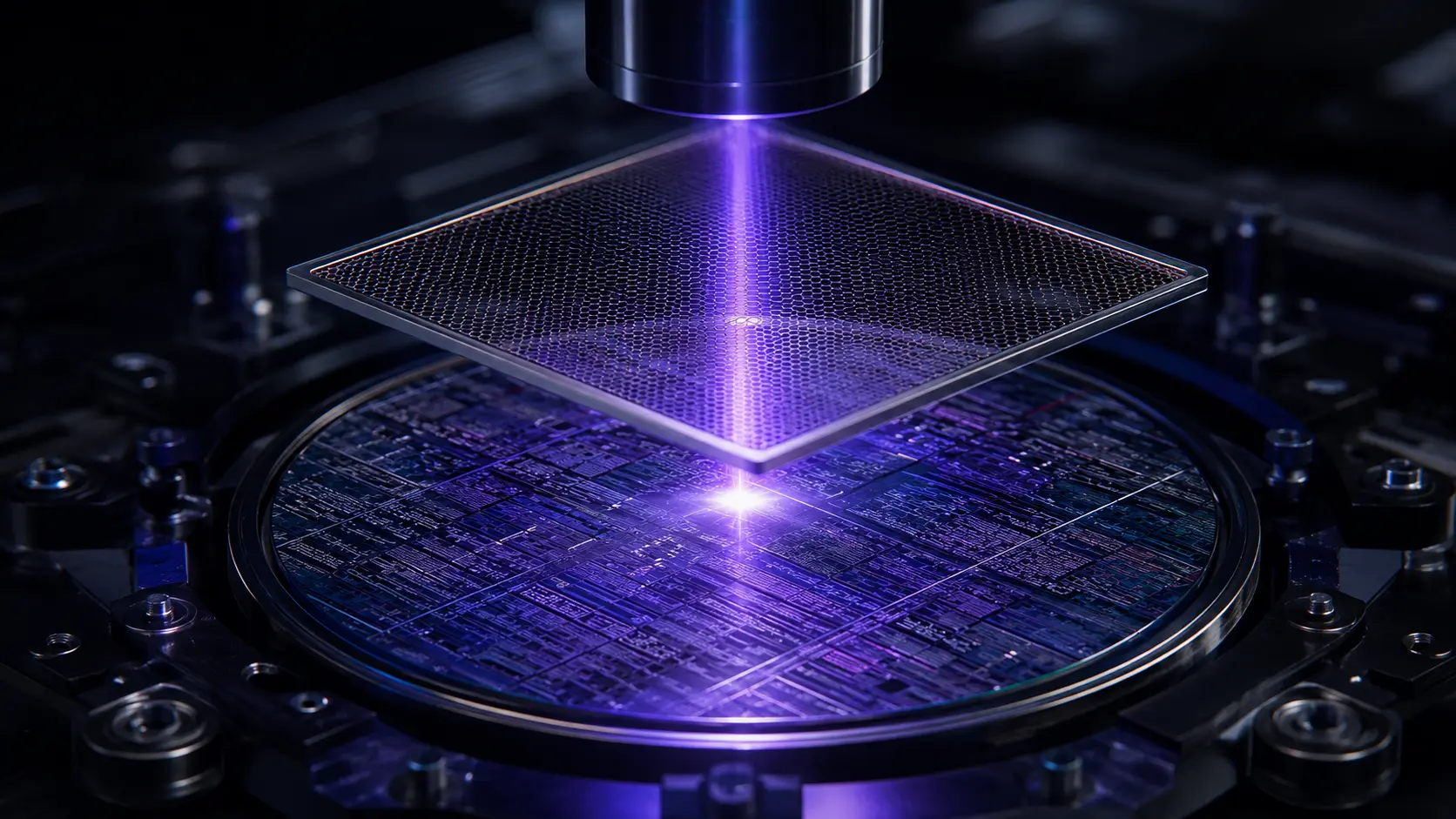
To print modern microchips, foundries bounce Extreme Ultraviolet (EUV) light off a mirror-like stencil called a reticle. Because the features are the size of individual atoms, a single speck of dust falling on this stencil ruins the printed pattern. If the stencil prints a ruined pattern onto the silicon wafer, every subsequent chip in that batch fails permanently.
Foundries historically protected these stencils using a pellicle—a transparent dust cover. However, EUV light operates at a wavelength of 13.5 nanometers. At this specific frequency, the light physically absorbs into almost every known material on Earth, including air and traditional glass. This forces engineers to manufacture pellicle membranes out of exotic materials just a few dozen atoms thick.
When an EUV scanner fires a 400-watt beam of light through this microscopic membrane, the pellicle absorbs a fraction of that energy as intense kinetic heat. Traditional polysilicon materials simply melt or warp under this thermal load. A warped pellicle instantly bends the light passing through it, distorting the transistor pattern and destroying the chip’s electrical geometry.
To survive this extreme environment, chemical engineers synthesize pellicles using networks of Carbon Nanotubes (CNTs). These microscopic carbon cylinders form a porous, incredibly strong web. The physical geometry of the CNT matrix allows over ninety percent of the EUV light to pass through unobstructed, while its high thermal conductivity rapidly disperses the absorbed heat before the membrane can mechanically deform.
WHY IT MATTERS NOW
The global semiconductor industry is aggressively shifting to High-Numerical Aperture (High-NA) EUV lithography to break the 2-nanometer barrier. These new machines require light sources pushing well past 400 watts to maintain profitable wafer-processing speeds. As the optical power increases, the thermal stress on the pellicle scales exponentially.
If a foundry cannot source a pellicle capable of surviving 400 watts, it faces a brutal operational paradox. It must either lower the power of its multi-million-dollar ASML scanner—directly halving its factory output—or run the machine without a pellicle entirely. Running without a pellicle requires halting the machine constantly to physically inspect and clean the stencil, destroying the unit economics of the entire fabrication plant.
Samsung recently demonstrated this exact vulnerability when it struggled with early 3-nanometer yield rates. While the industry fixated on new transistor gate designs, a major hidden factor was pellicle transmission efficiency. High defect rates on unprotected reticles force foundries to throw away thousands of ruined chips, rapidly erasing their financial margins.
The carbon nanotube pellicle solves this capital efficiency crisis. By supplying a membrane that survives extreme thermal environments without optical distortion, chemical suppliers dictate the actual, real-world throughput of a sovereign nation’s semiconductor infrastructure. The materials science of this nanometer-thick film directly regulates the global supply of artificial intelligence accelerators.
WHAT MOST PEOPLE MISS
Industry analysts frequently track the shipment of ASML lithography machines as the ultimate metric of global semiconductor capacity. They entirely miss that the pellicle acts as the physical and financial speed limit for the entire factory. A 350-million-dollar lithography tool cannot operate at its advertised capacity if the 30,000-dollar consumable membrane inside it melts under peak power.
Furthermore, foundries do not just worry about the pellicle blocking the light; they fear the pellicle outgassing. When intense EUV energy hits a composite membrane, trace chemical impurities in the material can vaporize. This vapor coats the highly expensive, perfectly polished Zeiss mirrors inside the scanner, permanently blinding the optics and causing hundreds of millions of dollars in catastrophic hardware damage.
THE TRAJECTORY
Next 12–36 Months: Major foundries will establish baseline 400W EUV manufacturing using dense CNT pellicles. Material suppliers will optimize the carbon matrix to consistently achieve 94% light transmission, heavily reducing the optical penalty of using a dust cover and instantly boosting sub-3nm wafer throughput.
Next Five Years: The integration of specialized metallic capping layers. Engineers will coat the raw carbon nanotubes with trace amounts of ruthenium or molybdenum. This microscopic metallic armor will protect the carbon from the highly reactive hydrogen plasma environment inside the scanner, extending the pellicle’s operational lifespan from weeks to months.
Next Ten Years: The realization of dynamic electromagnetic particle deflection. As light sources approach 1000 watts for next-generation nodes, no physical material will survive the thermal load. Foundries will replace physical pellicles with active electromagnetic fields that detect and physically repel microscopic dust particles away from the reticle in real time.
What Could Go Wrong: Severe acoustic resonance failure. A modern EUV scanner moves the reticle back and forth with extreme physical violence, accelerating at forces exceeding 10 Gs. If the surrounding vacuum environment fluctuates, the fragile pellicle membrane can catch the air pressure wave, vibrating violently until it mechanically shatters across the expensive optics.
Most Likely Outcome: Carbon nanotube pellicles will firmly establish themselves as the irreplaceable consumable of the sub-2nm era. The specialized chemical corporations that master the high-volume synthesis of these membranes will capture massive, recurring profit margins from every major logic foundry on Earth.
KEY TERMS
- EUV Lithography: A highly advanced manufacturing process using extreme ultraviolet light to print microscopic circuits onto silicon wafers.
- Reticle: The perfectly polished master template that holds the physical blueprint of the microchip pattern.
- Pellicle: An ultra-thin, transparent membrane stretched across a frame to catch falling dust particles before they hit the reticle.
- Carbon Nanotube (CNT): A microscopic cylindrical molecule of pure carbon possessing extreme physical strength and exceptionally high thermal conductivity.
- Transmission Efficiency: The exact mathematical percentage of EUV light that successfully passes through a pellicle without being absorbed or deflected.
SOURCES
- SPIE (International Society for Optics and Photonics) — Carbon Nanotube Pellicles for High-Volume EUV Lithography
- ASML — Pellicle Transmission and Thermal Load Management in High-NA EUV Scanners
- Imec — Advanced Materials for EUV Pellicle Mechanical and Thermal Resilience
- Journal of Micro/Nanopatterning, Materials, and Metrology — Hydrogen Plasma Etching and Metallic Capping of CNT Pellicles