Advertisement
)

AT A GLANCE
- Concept: Monolithic Die: The traditional method of manufacturing an entire processor as one single, continuous piece of silicon.
- Concept: Yield Rate: The percentage of chips on a silicon wafer that actually work without microscopic defects.
- Concept: Interposer: A foundational layer of silicon that acts as a microscopic high-speed bridge between different chiplets.
- Concept: UCIe: Universal Chiplet Interconnect Express, the standardized language that allows chiplets from different manufacturers to communicate.
IN SIMPLE WORDS
Imagine building a massive, highly detailed LEGO castle. If you had to mold the entire castle out of one giant piece of plastic, a single tiny air bubble would ruin the whole model. You would have to throw it away and start over, making the process incredibly expensive.
For decades, the computer industry built microchips exactly this way. They printed increasingly massive “monolithic” chips. As these chips grew larger to handle artificial intelligence, the chance of a microscopic dust particle ruining the entire chip skyrocketed.
To fix this, engineers stopped building the whole castle at once. Instead, they manufacture the individual blocks separately—one for memory, one for graphics, one for math. If one block is broken, they throw away just that tiny block, not the whole processor. They then glue the perfect blocks together on a microscopic foundation, creating a mega-chip that is vastly cheaper and more powerful than a single piece of silicon could ever be.
HOW CHIPLET ARCHITECTURE WORKS
The semiconductor industry is fighting the physical limits of Moore’s Law. Printing billions of transistors on a single monolithic die forces the silicon footprint to expand. As the die size approaches the reticle limit—the maximum physical area a lithography machine can expose at once—manufacturing yield rates plummet.
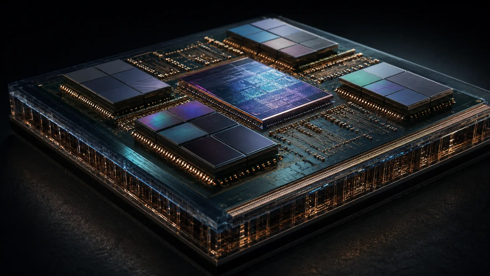
Chiplet architecture solves this by disaggregating the processor. Instead of one massive System-on-Chip (SoC), engineers design smaller, discrete logic blocks called chiplets. Because these individual pieces are small, the probability of a random manufacturing defect destroying them is mathematically much lower. This exponentially increases the number of usable chips harvested from a single silicon wafer.
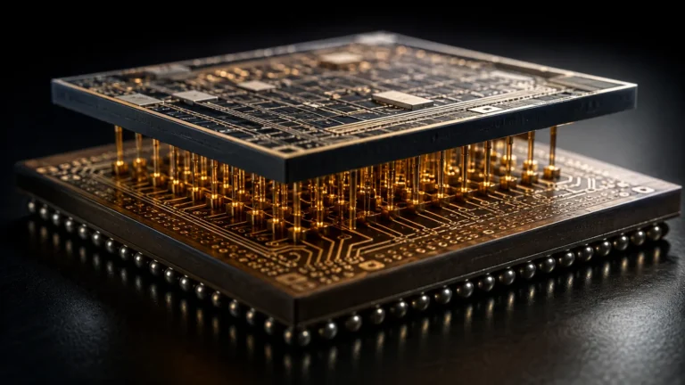
To function as a unified processor, these independent chiplets must be physically connected. Engineers place the chiplets onto an interposer, a base layer of silicon embedded with microscopic wiring. Through-Silicon Vias (TSVs) run vertically through the interposer to supply power, while dense horizontal micro-bumps allow the chiplets to instantly share data at massive bandwidths.
The communication between these blocks is governed by advanced packaging protocols. Historically, every manufacturer used proprietary connection logic. Today, the industry is standardizing around the Universal Chiplet Interconnect Express (UCIe). This open standard acts as a universal translator, dictating the physical layer and data protocols required to move bits across the interposer with near-zero latency.
Because of UCIe, chiplet architecture allows for aggressive node mixing. A company does not need to manufacture its entire processor on an ultra-expensive 3-nanometer node. It can print the high-performance math cores on 3nm, while printing the less critical input/output (I/O) controllers on a much cheaper, older 12nm node. They stitch the mismatched pieces together on the interposer, drastically reducing total production costs while maintaining peak performance.
REAL WORLD EXAMPLE
AMD successfully utilized chiplet architecture to rescue its server market share from Intel. With their EPYC processor line, AMD stopped trying to print one massive, expensive server chip.
Instead, they designed a central I/O die and surrounded it with up to twelve smaller “Core Complex Dies.” If a customer wanted a cheaper processor, AMD simply glued fewer core chiplets onto the package. This modular approach allowed AMD to rapidly scale core counts far beyond what a monolithic chip could support, severely undercutting competitors on price and fundamentally altering the economics of data center hardware.
WHY IT MATTERS NOW
The absolute demand for artificial intelligence compute is forcing processors to scale beyond traditional physical limits. Massive AI training models require processors packed with High-Bandwidth Memory (HBM) and thousands of tensor cores. A single monolithic chip physically cannot hold enough transistors to meet this demand without breaking the lithographic reticle limit.
Chiplets provide the only mathematical escape route. By stitching multiple dies together via 2.5D and 3D packaging, foundries can build processors that are functionally larger than the machines that print them. This architecture is the primary reason hardware companies can continue scaling AI performance year over year.
This shift fundamentally rewrites semiconductor supply chains. Historically, chip design and manufacturing were vertical silos. Now, a hardware company can purchase a memory chiplet from SK Hynix, a logic chiplet from TSMC, and an I/O chiplet from GlobalFoundries, assembling them into a custom package.
The strategic chokepoint has officially moved from simply printing the silicon to packaging it. The ability to flawlessly align tens of thousands of microscopic copper pillars between a chiplet and an interposer is now the most highly sought-after engineering capability in the global tech economy.
COMMON MISCONCEPTIONS
- “Chiplets are completely new technology.” Multi-chip modules have existed for decades. What is new is the extreme density of the modern micro-bumps and the ability to move terabytes of data between the chips with almost zero latency or power penalty.
- “Chiplets make the processor physically smaller.” Chiplets actually make the final packaged processor larger and thicker. The advantage is in the modularity and cost-saving yield rates, not the final physical footprint.
- “You can snap them together like real LEGOs.” Chiplets must be bonded in hyper-clean environments using advanced thermocompression or hybrid bonding techniques. Once attached to the interposer, they are permanently fused and cannot be swapped out later.
WHAT MOST PEOPLE MISS
Hardware analysts obsess over the connection speed between the chiplets, but they frequently overlook the massive thermodynamic crisis this architecture creates.
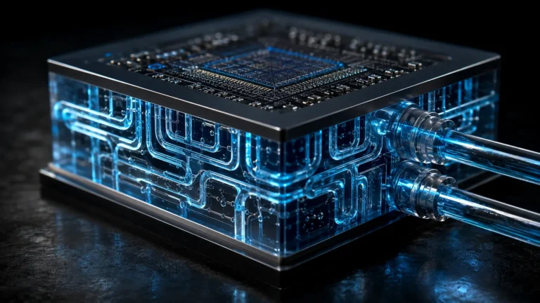
When you pack multiple high-performance chiplets mere millimeters apart on a single interposer, you create extreme, highly localized thermal density. The heat generated by the central logic chiplets cannot easily escape because it is surrounded by other heat-generating blocks. If packaging engineers cannot design microscopic liquid cooling channels or advanced heat spreaders directly into the interposer, the entire mega-chip will thermally throttle, erasing the performance gains of the architecture.
THE ECONOMIC AND STRATEGIC IMPACT
The immediate financial winner is TSMC, which currently holds a virtual monopoly on advanced packaging through its CoWoS (Chip-on-Wafer-on-Substrate) technology. Companies designing high-end AI accelerators are entirely dependent on TSMC’s packaging capacity, giving the Taiwanese foundry absolute pricing power over the AI hardware market.
For semiconductor startups, the UCIe standard acts as an economic equalizer. A small startup no longer needs to spend $500 million designing an entire monolithic processor. They can focus solely on designing one highly specialized AI accelerator chiplet, relying on standard off-the-shelf chiplets for memory and I/O. This drastically lowers the barrier to entry for silicon innovation.
Geopolitically, advanced packaging offers a backdoor for nations facing export controls. If a nation cannot acquire extreme ultraviolet (EUV) lithography machines to print 3nm chips, they can compensate by using advanced packaging to densely stack dozens of older, domestically produced 14nm chiplets. This creates a mega-chip capable of rivaling modern processors, partially bypassing international trade restrictions.
THE TRAJECTORY
Next 12–36 Months: The stabilization of the UCIe standard will spawn a commercial “chiplet marketplace.” Hardware vendors will begin selling pre-validated, un-packaged silicon blocks, allowing companies to assemble custom mega-chips by ordering parts from an open catalog.
Next Five Years: The dominance of 3D hybrid bonding. Instead of placing chiplets side-by-side on a 2.5D interposer, foundries will aggressively stack active logic chiplets directly on top of each other. This vertical stacking will reduce data travel distance to micrometers, vastly increasing processing speed and energy efficiency.
Next Ten Years: The deployment of silicon photonics in chiplet packaging. Engineers will replace internal copper wiring with microscopic optical waveguides. Chiplets will communicate with each other using pulses of light, virtually eliminating heat generation from data transfer and allowing processors to scale to unprecedented sizes.
What Could Go Wrong: A severe substrate shortage. The organic materials and specialized glass used to build the foundational layers beneath the interposer are produced by a very small group of chemical suppliers. A supply chain disruption in these obscure raw materials would instantly halt the production of all advanced chiplet processors globally.
Most Likely Outcome: Monolithic processor design will be completely abandoned for all high-performance computing. Chiplet architecture, supported by universal interconnect standards, will become the permanent blueprint for the semiconductor industry, sustaining the trajectory of computational power for the next two decades.
KEY TERMS
- Chiplet: A small, specialized piece of silicon designed to be combined with other chips to form a larger, unified processor.
- Monolithic Die: A traditional processor manufactured as a single, continuous piece of silicon.
- Yield Rate: The percentage of usable, defect-free chips harvested from a manufactured silicon wafer.
- Interposer: A foundational layer that sits beneath the chiplets, filled with microscopic wires that route data and power between them.
- UCIe (Universal Chiplet Interconnect Express): An open industry standard defining how chiplets from different manufacturers physically connect and communicate.
- Reticle Limit: The maximum physical dimensions a lithography machine can print onto a silicon wafer in a single exposure.
- Advanced Packaging: The complex engineering process of securely connecting multiple chiplets, interposers, and memory stacks into a final processor housing.
BEGINNER FAQ
What is a chiplet? It is a small, specialized microchip. Instead of making one giant processor to do everything, engineers make several small chiplets and link them together to act as one large brain.
Why did companies stop making one giant chip? As chips get bigger, the chance of a microscopic mistake ruining the whole piece of silicon increases. Making smaller pieces and throwing away the broken ones is much cheaper.
How do the pieces talk to each other? They are placed onto a foundation called an interposer, which contains thousands of microscopic wires. These wires allow the chiplets to share data instantly.
Can you mix and match different brands of chiplets? Historically, no. But the industry is adopting a new rulebook called UCIe. This standard ensures that a chiplet from one company can physically connect to a chiplet from another company.
Why is this important for artificial intelligence? AI requires massive amounts of computing power. We physically cannot print a single chip big enough to handle it anymore. Chiplets allow us to glue multiple chips together to meet the demand.
Does this make the computer faster? Yes. By putting the memory chiplets incredibly close to the math chiplets on the same foundation, the data travels a shorter distance, making the whole processor calculate faster.
What is advanced packaging? It is the highly complex factory process of perfectly aligning and gluing all these tiny chiplets together without breaking them or disrupting the microscopic wires.
Is this only for expensive supercomputers? While it started in high-end data centers, the cost savings of chiplets mean this design is rapidly becoming the standard for consumer laptops and gaming consoles.
SOURCES
- Institute of Electrical and Electronics Engineers (IEEE) — Heterogeneous Integration and Chiplet Architecture Scaling
- Universal Chiplet Interconnect Express (UCIe) Consortium — Interconnect Specifications and Open Silicon Ecosystems
- Taiwan Semiconductor Manufacturing Company (TSMC) — 3DFabric and CoWoS Advanced Packaging Technology
- Semiconductor Industry Association (SIA) — Post-Moore’s Law Hardware Trajectories and Advanced Packaging