Advertisement
)

At a Glance
Concept: Extremely precise physical measurement of silicon wafer components during manufacturing.
Why it matters: Errors the size of a few atoms can destroy an entire microchip.
Who uses it: Global semiconductor foundries like TSMC, Intel, and Samsung.
Biggest takeaway: Manufacturing advanced AI chips is impossible without metrology guiding the lithography lasers.
In Simple Words
Imagine trying to build a massive city out of Lego bricks, but the entire city must fit on a surface the size of your fingernail. To do this successfully, you would need a ruler capable of measuring fractions of a millimeter.
Semiconductor metrology provides that ruler for the microchip industry.
Modern computer chips contain billions of tiny electrical switches called transistors. These transistors are now so small they are measured in nanometers—a scale approaching the size of individual atoms. You cannot manufacture what you cannot measure.
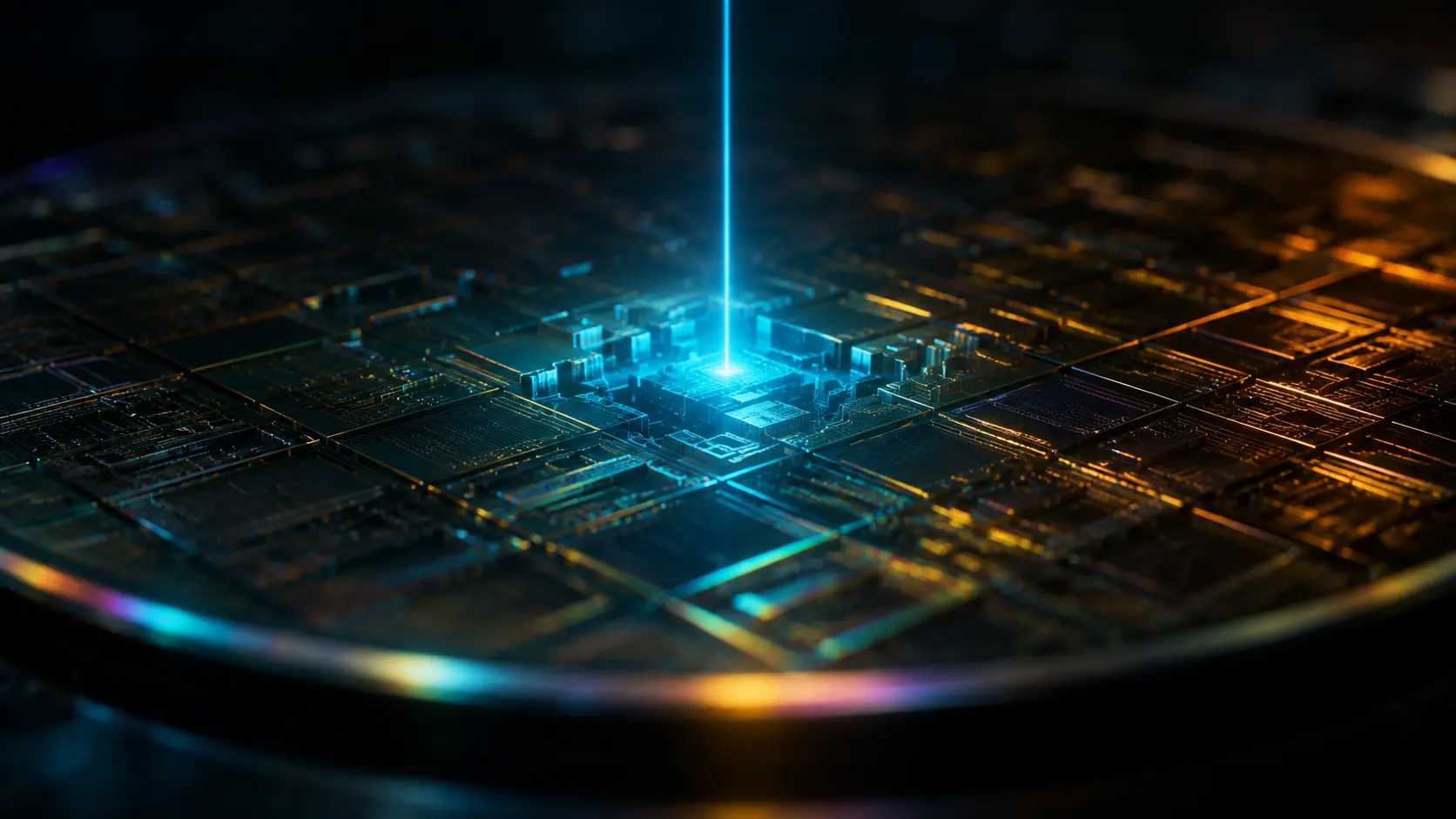
Metrology uses incredibly advanced tools, such as electron beams and highly focused lasers, to inspect these tiny structures as they are being built. It checks if the microscopic wires are too thin, if a transistor is slightly misplaced, or if a single speck of dust has ruined the circuit. Without this constant measurement and feedback, building modern smartphones or artificial intelligence systems would be physically impossible.
Why This Matters
The global economy is currently experiencing an unprecedented demand for computational power. Artificial intelligence, autonomous vehicles, and advanced defense systems all rely on processors operating at the 3-nanometer (nm) node and below.
At this microscopic scale, the laws of classical physics begin to blur with quantum mechanics. In a semiconductor megafab, building a chip involves hundreds of sequential chemical, optical, and etching steps applied to a single silicon wafer. If a microscopic alignment error occurs at step 10, and it is not caught until step 500, the foundry has just wasted weeks of expensive manufacturing time and materials. Metrology provides the critical feedback loop that prevents this cascading failure.
Economically, the stakes are staggering. A state-of-the-art semiconductor manufacturing facility costs upwards of $20 billion to construct. The profitability of that facility depends entirely on its “yield”—the percentage of working chips produced per wafer. If a fab operates with a yield of 50%, it loses money. If it can push that yield to 90%, it generates billions in profit. Metrology is the primary engineering discipline that enables technicians to identify defects, tweak the manufacturing parameters, and drive yield upwards.
Strategically, metrology tools represent a massive geopolitical chokepoint. Just as nations restrict the export of the lithography machines that print the chips, they also restrict the export of the advanced metrology machines required to measure them. Controlling the global supply of high-end measurement equipment allows allied nations to throttle the technological advancement of strategic adversaries, cementing metrology as a pillar of national security.
HOW SEMICONDUCTOR METROLOGY WORKS
Measuring a 3-nanometer transistor requires bypassing the limits of human vision. Visible light has a wavelength of about 400 to 700 nanometers. Trying to measure a 3nm transistor with visible light is like trying to measure the grooves on a vinyl record using a basketball.
Metrology must use waves smaller than the object being measured.
1. Critical Dimensions and Overlay: The two most important metrics in a fab are Critical Dimension (CD) and Overlay. CD is the exact physical width of a printed line or transistor gate. Overlay is the exact alignment of one layer of circuitry on top of the previous layer. If a wire on layer two does not perfectly hit the contact pad on layer one, the chip shorts out and dies.
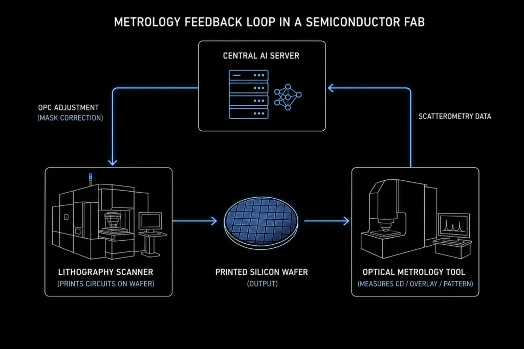
2. Optical Metrology and Scatterometry: For rapid, high-volume measurement, fabs use Optical Critical Dimension (OCD) tools. Because visible light is too large to resolve the image, these tools do not take a traditional picture. Instead, they use a technique called scatterometry.
The machine fires a broad beam of light at a specialized grating pattern printed on the edge of the wafer. The light bounces off the pattern and scatters, returning to the sensor as a complex diffraction signature. A supercomputer instantly compares this raw mathematical signature against millions of simulated models. By finding the exact match, the system mathematically deduces the exact physical shape, height, and width of the printed structure.
3. Electron-Beam Metrology (CD-SEM): When optical scatterometry is not precise enough, engineers turn to a Critical Dimension Scanning Electron Microscope (CD-SEM). Electrons have a wavelength exponentially smaller than light, allowing them to resolve individual atoms.
A CD-SEM fires a high-voltage beam of primary electrons directly at the silicon wafer. When these primary electrons strike the surface, they knock secondary electrons out of the silicon atoms. Highly sensitive detectors catch these escaping secondary electrons. A computer analyzes the trajectory and volume of the secondary electrons to rebuild a perfect, high-resolution 3D topographical map of the transistor.
4. Optical Proximity Correction (OPC): Metrology data is useless if it is not acted upon. The measurement data is instantly fed back into the fab’s central control server.
If the CD-SEM detects that the edges of a printed microscopic wire are rounding off instead of printing sharply, the server sends a command to the lithography machine. The lithography software uses Optical Proximity Correction (OPC) to alter the shape of the light mask for the very next wafer. It intentionally distorts the projected image so that the optical physics cancel out the error, forcing the wire to print perfectly straight on the silicon.
5. System Limitations: The fundamental limitation of semiconductor metrology is the brutal trade-off between speed and resolution.
Optical metrology is fast enough to measure thousands of wafers an hour, but it struggles to resolve complex 3D structures at the atomic level. Electron-beam metrology provides perfect atomic resolution, but it is incredibly slow. Scanning an entire 300mm silicon wafer with a single electron beam would take years. Therefore, engineers must rely heavily on statistical sampling, only measuring tiny fractions of the wafer and hoping those measurements accurately represent the entire batch.
Real-World Applications
Advanced measurement tools are deployed constantly throughout the semiconductor supply chain.
EUV Lithography Alignment: ASML’s Extreme Ultraviolet (EUV) lithography machines rely heavily on internal metrology sensors. To print sub-3nm chips, the machine must align its internal mirrors within picometers (trillionths of a meter). Metrology lasers constantly measure the mirror positions to ensure the 13.5nm EUV light hits the exact correct coordinate on the silicon wafer.
Wafer Defect Inspection: Companies like KLA build specialized optical defect inspectors. These machines scan a moving 300mm silicon wafer in minutes, hunting for “killer defects.” If a microscopic dust particle or a drop of rogue chemical is identified on the wafer, the metrology tool halts the line so the wafer can be chemically washed before the defect is permanently baked into the next layer of the chip.
3D NAND Flash Memory: Modern solid-state hard drives (NAND flash) stack over 200 layers of circuitry vertically. To connect these layers, manufacturers must drill microscopic trenches straight down through all 200 tiers. Advanced metrology tools use deep-penetrating infrared light to measure the depth and straightness of these microscopic canyons, ensuring the top layer connects flawlessly to the bottom layer.
Economic & Strategic Impact
The metrology market dictates the pace of global computational progress.
For businesses, the companies providing these tools—such as KLA, Applied Materials, ASML, and Hitachi High-Tech—command massive economic power and high profit margins. Foundry operators like TSMC, Samsung, and Intel spend billions of dollars annually on metrology equipment because catching a systemic defect one hour earlier saves tens of millions of dollars in ruined silicon.
For governments, metrology is a critical lever in trade warfare. Developing a domestic semiconductor industry is impossible without the tools to measure the output. By restricting the export of sub-nanometer metrology equipment, Western governments effectively prevent adversarial nations from successfully scaling high-yield artificial intelligence hardware manufacturing.
For the global market, investors track the quarterly sales of metrology tools as a leading economic indicator. High metrology equipment sales signal that major foundries are successfully moving past the research phase and are aggressively ramping up production of entirely new, complex chip architectures.
Advantages
Yield Maximization: Identifies microscopic errors early in the 500-step manufacturing process, preventing billions of dollars in wasted materials.
Automated Feedback: Allows megafabs to operate 24/7, with software automatically correcting printer drift without human intervention.
Atomic Visibility: Pushes human engineering past the limits of visible light, enabling the continuation of Moore’s Law and cheaper computing.
Limitations
Throughput Bottlenecks: The most accurate electron-beam tools are far too slow to inspect every chip, forcing reliance on statistical guessing.
Destructive Testing: Some deep measurements require cutting a finished wafer open (cross-sectioning) to see the bottom layers, which physically destroys the product.
Extreme Sensitivity: Metrology machines are so precise that they must be heavily isolated; a truck driving on a highway a mile away can create enough seismic vibration to ruin a scan.
Common Misconceptions
Misconception: Metrology is just quality control at the very end of the assembly line.
Reality: Metrology happens continuously during the build process. A wafer may visit a metrology station thirty times before the chip is actually finished, providing active, real-time corrections to the machines.
Misconception: Engineers use powerful optical microscopes to look at transistors.
Reality: Modern transistors are smaller than the wavelength of visible light. They are physically invisible to traditional optics. They can only be “seen” using electrons, X-rays, or complex mathematical light scattering.
Misconception: Every single microchip is measured before it is sold.
Reality: Fabs use statistical sampling. They measure specific test patterns printed on the very edges of the wafer. Measuring every individual transistor would take longer than the lifespan of the universe.
What Most People Miss
The true bottleneck in semiconductor metrology is not optics or lasers—it is raw computing power.
When an optical scatterometry tool fires light at a wafer and receives a complex diffraction pattern back, that raw light data is useless to a human engineer. The machine must instantly compare that specific light pattern against millions of mathematically simulated 3D models to find a match.
Modern metrology tools are essentially massive supercomputers attached to high-end sensors. Today, equipment manufacturers heavily utilize machine learning and artificial intelligence to speed up this pattern-matching process. The ultimate irony of the semiconductor industry is that AI is now absolutely required to measure and manufacture the chips that will eventually run AI.
Comparison Table
| Feature | Optical Scatterometry (OCD) | Electron-Beam Metrology (CD-SEM) |
| Purpose | Rapid, high-volume measurement of overall shapes. | Perfect, high-resolution imaging of individual structures. |
| Measurement Method | Analyzes how light waves scatter and diffract. | Fires electrons and measures the secondary particle response. |
| Speed / Throughput | Extremely fast (hundreds of wafers per hour). | Extremely slow (fractions of a wafer per hour). |
| Resolution | Limited by the wavelength of light. | Sub-nanometer (can resolve individual atoms). |
| Damage to Wafer | Non-destructive. | High-energy electron beams can occasionally damage delicate photoresists. |
| Cost | High. | Very High. |
| Best Fit | Continuous inline mass-production feedback. | Research, development, and diagnosing new, unknown defects. |
Case Study
Situation: A leading global semiconductor foundry was transitioning from the 5-nanometer process node down to the highly complex 3-nanometer node.
Challenge: At 3nm, the transistors were packed so tightly together that traditional optical metrology tools could no longer cleanly resolve the physical gap between them. The light waves were simply too thick, returning messy data. This caused the fab’s yield to stall at an unprofitable 40%, threatening their ability to fulfill massive orders for a major smartphone manufacturer.
Solution: The foundry integrated a new generation of multi-beam SEM technology alongside AI-driven scatterometry. Instead of using a single electron beam, the new tool fired 64 tiny electron beams simultaneously, drastically increasing the scanning speed while maintaining atomic resolution.
Outcome: The AI system used the high-resolution multi-beam data to actively calibrate the faster optical tools in real-time. This hybrid approach allowed the foundry to identify the specific lithography misalignment causing the failures. Yields rapidly increased past 85%.
Lessons Learned: No single metrology tool can solve advanced node manufacturing. The foundry with the best software integration—blending the speed of optics with the accuracy of electrons—wins the race to commercialize the next generation of microchips.
Future Outlook
Next 12–24 Months: Artificial intelligence will take over the defect classification process. Instead of human technicians reviewing flagged anomalies, neural networks will instantly classify defects, determine their root chemical cause, and autonomously alter fab machinery parameters to fix the issue in real-time.
Next 3–5 Years: The industry will transition toward “inline” metrology. Currently, a wafer must be removed from a vacuum processing chamber and carried to a separate metrology machine. New tools will integrate sensors directly inside the plasma etching chambers, measuring the transistors at the exact millisecond they are being carved into the silicon.
Next 10 Years: As the industry pushes toward 1-nanometer architectures and complex 3D-stacked transistors (Gate-All-Around), standard electrons will not penetrate deeply enough. Metrology will heavily adopt compact, lab-scale X-ray scattering tools, using highly energetic X-rays to see straight through hundreds of layers of solid silicon simultaneously.
Most Likely Scenario: The cost of metrology equipment will continue to skyrocket, matching the cost of the lithography machines themselves. This massive capital requirement will further consolidate the semiconductor industry, leaving only two or three mega-foundries on Earth financially capable of manufacturing the most advanced microchips.
Key Takeaways
Metrology is the science of precise measurement required to build sub-nanometer computer chips.
Without metrology feedback loops, microscopic errors would ruin every silicon wafer manufactured.
Critical Dimension (CD) and Overlay are the two most important measurements for transistor viability.
Optical scatterometry uses light diffraction patterns to measure structures rapidly at high volumes.
Scanning Electron Microscopes (CD-SEM) use electrons to provide slow, but perfect, atomic-level resolution.
Optical Proximity Correction (OPC) uses metrology data to intentionally distort light masks to print perfectly.
Controlling advanced metrology tools gives nations significant geopolitical leverage over global computing power.
Glossary
Critical Dimension (CD): The exact, specified physical width of a microscopic feature, such as a wire or transistor gate, printed on a silicon wafer.
CD-SEM (Critical Dimension Scanning Electron Microscope): A specialized tool that uses a focused beam of electrons to measure semiconductor features with atomic precision.
EUV (Extreme Ultraviolet) Lithography: The machine that prints the microchips using 13.5nm wavelength light, relying heavily on metrology for alignment.
Metrology: The scientific study of measurement; in semiconductors, it refers to the tools and processes used to inspect wafers.
Optical Proximity Correction (OPC): A software technique that pre-distorts the shapes on a lithography photomask to compensate for physical light-scattering errors.
Overlay: The precise vertical alignment between two different layers of circuitry on a microchip.
Scatterometry: A non-destructive optical measurement technique that deduces the shape of an object by analyzing how it scatters a beam of light.
Yield: The percentage of fully functional, sellable microchips produced on a single silicon wafer.
Frequently Asked Questions
Why is measuring a microchip so difficult? Modern transistors are smaller than a human virus and smaller than the wavelength of visible light. You cannot use standard microscopes; you must use incredibly complex electron beams or mathematically deduce shapes using scattered light.
What happens if a metrology machine makes a mistake? The fab’s central server relies on that data to calibrate the manufacturing equipment. A false measurement will cause the lithography machines to misalign the next batch of wafers, potentially ruining millions of dollars of inventory in minutes.
How long does it take to measure a silicon wafer? Optical tools can measure a wafer in a few minutes. High-resolution electron-beam tools might take an hour just to measure a few isolated test patterns on the wafer. Speed is the primary bottleneck.
Do they measure the actual chip you buy in the store? Usually, no. Because measuring takes time, engineers print specialized “metrology targets” (tiny test shapes) on the outer edges of the wafer. They measure the test targets and mathematically assume the main chips printed similarly.
Can metrology see inside the solid silicon? Standard electron beams only see the surface. To see inside, engineers either physically slice the chip open (destructive testing) or use highly advanced infrared and X-ray metrology to peer through the layers.
Why does the metrology equipment cost so much? The machines require perfect vacuum chambers, vibration isolation systems that float on magnetic fields, and lasers calibrated to the picometer. The physics required simply cannot be mass-produced cheaply.
What is a “killer defect”? It is a microscopic flaw—like a stray dust particle or an incomplete chemical etch—that physically shorts out a wire, rendering the entire microchip permanently dead.
How does artificial intelligence help metrology? Optical tools gather messy light reflections and must compare them against millions of simulated 3D models to find the correct shape. AI pattern-matching algorithms do this instantly, allowing the machines to operate at factory speeds.
Sources
National Institute of Standards and Technology (NIST): Nanoscale Metrology Group
SEMI (Semiconductor Equipment and Materials International): Yield Management and Metrology Reports
SPIE (The International Society for Optics and Photonics): Advanced Lithography and Patterning
KLA Corporation: Advanced Wafer Inspection and Metrology Technical Publications