Advertisement
)

At a Glance
- Concept: Replacing electrical copper wiring with microscopic optical laser channels inside computer chips.
- Why it matters: Artificial intelligence and cloud data centers are suffocating under the heat and speed limits of traditional electrical wiring.
- Who uses it: Cloud infrastructure providers, telecom networks, and advanced semiconductor foundries.
- Biggest takeaway: The future of high-performance computing relies on integrating optical physics natively into standard silicon manufacturing.
In Simple Words
Inside every computer, data travels as electrical pulses through microscopic copper wires. For decades, this system worked perfectly. But today, computers are processing massive amounts of data for artificial intelligence, and copper is hitting a physical wall. If you push too much electricity through a copper wire too fast, it generates intense heat and the data signal degrades.
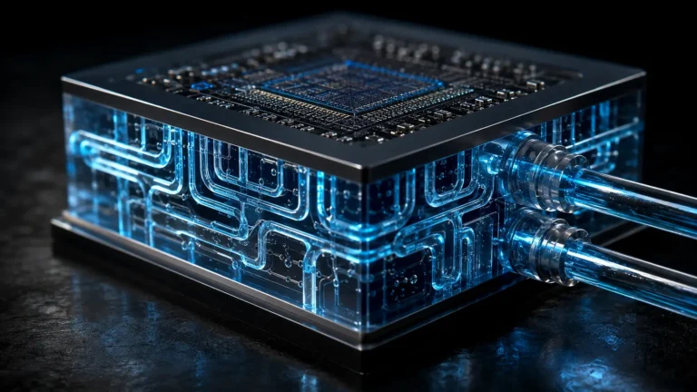
To fix this, engineers developed silicon photonics. Instead of sending electrical pulses through copper, they shoot microscopic lasers through tiny, glass-like channels carved directly into the silicon chip.
Because light moves faster than electricity, generates almost no heat, and does not degrade over short distances, it allows computer chips to communicate at speeds that were previously impossible. It is the equivalent of upgrading a city’s congested, single-lane dirt road into an instant, frictionless teleportation network.
Why This Matters
The technology industry is currently facing a silent crisis known as the I/O (Input/Output) bottleneck.
Modern processors, specifically the Graphics Processing Units (GPUs) used to train artificial intelligence, have become incredibly fast at performing mathematical calculations. However, an AI model cannot be trained on a single chip; it requires tens of thousands of processors working together in a massive data center. These chips must constantly share data with one another to function as a unified supercomputer.
The problem is that the copper cables connecting these chips cannot keep up with the processing speed. The processors spend a massive amount of time simply waiting for data to arrive. To speed up the copper wires, engineers are forced to pump more electricity through them, which generates lethal amounts of heat. In a modern AI data center, cooling these electrical connections consumes an unsustainable percentage of the facility’s total power budget.
Silicon photonics completely rewires this architecture. By moving data with light, chips can communicate at peak velocities with virtually no thermal penalty.
This fundamentally changes how a data center is built. Today, servers must be physically placed close together because electrical signals die over long cables. With silicon photonics, a processor in one building can instantly share memory with a processor in another building as if they were sitting on the exact same motherboard. This breaks the physical constraints of hardware, allowing tech companies to build planetary-scale computing infrastructure.
HOW SILICON PHOTONICS WORKS
Moving light through a silicon chip requires shrinking massive fiber-optic telecom technology down to the microscopic level.
Here is exactly how engineers turn electrical data into light and move it across a microchip.
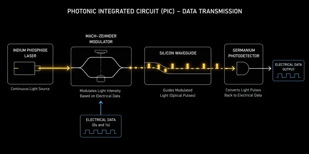
1. The Core Concept: Computers process data electronically (using electrons). Fiber-optic networks transmit data optically (using photons). Silicon photonics acts as a translator between these two domains. It converts the electrical ones and zeros of a computer processor into flashes of light, moves that light across a distance, and converts it back into electricity at the destination.
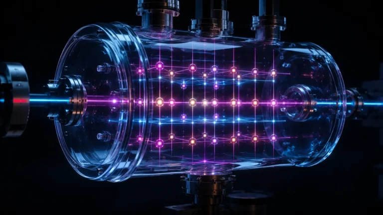
2. The Light Source: A fundamental physical problem is that silicon is an indirect bandgap semiconductor—meaning it cannot easily generate light on its own. To solve this, engineers must attach a tiny external laser, typically made from a different material like Indium Phosphide, directly to the silicon chip. This laser fires a continuous, steady beam of infrared light into the silicon.
3. Mach-Zehnder Modulators: To send data, that steady laser beam must be flickered on and off billions of times a second to represent ones and zeros. This is accomplished using a microscopic component called a Mach-Zehnder modulator.
The modulator splits the incoming laser beam into two separate paths. By applying a tiny electrical voltage to one of the paths, it alters the phase of the light wave. When the two paths recombine, the light waves either align and pass through (a “one”), or they crash into each other and cancel out, creating darkness (a “zero”). This happens seamlessly at billions of cycles per second.
4. Wave-Division Multiplexing (WDM): The pulsing light travels through microscopic channels etched into the silicon called waveguides. To maximize the amount of data traveling through a single waveguide, engineers use Wave-Division Multiplexing (WDM).
Instead of sending one beam of light, they send multiple different colors (wavelengths) of light through the exact same channel simultaneously. Because the colors do not interfere with one another, each wavelength can carry its own independent stream of data, exponentially increasing the bandwidth of the connection.
5. Photonic Integrated Circuits (PICs): The true breakthrough of silicon photonics is manufacturing. All of these complex optical components—the modulators, the waveguides, and the photodetectors that catch the light at the end—are carved into a single piece of silicon. This creates a monolithic Photonic Integrated Circuit (PIC). Because it uses standard silicon, it can be mass-produced in the exact same multibillion-dollar megafabs that already build standard computer chips, bringing the cost of optical technology down drastically.
6. System Limitations: The primary engineering challenge is alignment. The fiber-optic cables that carry the light out of the chip must be physically aligned to the microscopic silicon waveguides with atomic-level precision. A misalignment of a fraction of a micrometer causes the light to scatter and the signal to die. Securing these fragile optical connections so they survive the heat and vibration of a working data center requires highly complex, expensive packaging techniques.
Real-World Applications
Silicon photonics has transitioned from academic research into active deployment across critical global infrastructure.
Hyperscale Data Centers: Cloud providers like Amazon Web Services (AWS) and Google Cloud use millions of silicon photonics transceivers. These pluggable modules sit at the edges of server racks, taking the electrical data from the servers, converting it to light, and sending it through fiber-optic cables to other racks across the massive warehouse.
AI Supercomputer Networking: Training large language models requires moving petabytes of data continuously. NVIDIA and other AI hardware designers are embedding optical connections directly into their GPU clusters. This allows thousands of individual AI chips to act as a single, unified super-brain without being throttled by slow copper wiring.
Telecommunications Backhaul: The global rollout of 5G and 6G cellular networks requires moving massive amounts of data from local cell towers back to core internet hubs. Telecom providers use silicon photonics equipment to handle these heavy data loads efficiently, replacing older, bulky optical networking gear with tiny, silicon-etched chips.
Economic & Strategic Impact
The transition from electrons to photons dictates the economic viability of future technology sectors.
For data center operators, the shift represents a massive reduction in Total Cost of Ownership (TCO). Electrical interconnects require heavy cooling infrastructure. By replacing hot copper with cool light, facility operators can reclaim millions of dollars in electricity costs and allocate that power directly to the actual processors.
For the semiconductor industry, silicon photonics creates a highly lucrative sub-sector. Traditional foundries like TSMC, Intel, and GlobalFoundries are investing heavily in customized optical manufacturing lines. The companies that successfully master Co-Packaged Optics (CPO)—the ability to place the optical laser on the exact same substrate as the silicon processor—will dominate the next decade of hardware sales.
Strategically, overcoming the I/O bottleneck is a matter of national technological superiority. The nation that scales silicon photonics fastest will build the most capable artificial intelligence systems, as their supercomputers will not be constrained by the physical limitations of electrical wiring.
Advantages
Total Bandwidth Capacity
Light waves can carry exponentially more data than electrical signals. Using multiplexing, a single microscopic optical channel can move terabits of data per second, far exceeding the physical limits of standard copper wire.
Zero Signal Degradation
When electricity travels through copper, the signal degrades over distance due to resistance, requiring power-hungry amplifiers. Light traveling through high-quality waveguides and fiber optics experiences almost zero degradation, allowing perfect data transmission over long distances.
Thermal Efficiency
Electrical resistance generates heat, which is the primary enemy of computing. Photons do not generate meaningful friction or heat as they move, drastically reducing the cooling requirements of the hardware.
Manufacturing Scale
Because the optical components are etched into standard silicon wafers, they can be manufactured using the existing global infrastructure of semiconductor foundries, driving down costs through massive economies of scale.
Limitations
The Laser Material Problem
Silicon is excellent for routing light, but poor at generating it. Manufacturers must bond external lasers made from rare materials (like Indium Phosphide) to the silicon, adding significant complexity and cost to the manufacturing process.
Packaging Complexity
Connecting a standard glass fiber-optic cable to a microscopic silicon waveguide is an engineering nightmare. It requires highly specialized robotic alignment tools, making the final assembly of the chip a major production bottleneck.
High Initial Capital Costs
While mass production lowers the per-unit cost, redesigning a semiconductor foundry to handle optical components, specialized testing equipment, and new materials requires billions of dollars in upfront capital expenditure.
Common Misconceptions
Misconception: Silicon photonics means computers now use light to do math.
Reality: Computers still use electricity to perform mathematical logic (processing). Silicon photonics is strictly used for communication—moving the data between the processors and memory chips.
Misconception: It is just a smaller fiber-optic cable.
Reality: A fiber-optic cable is just a glass pipe. Silicon photonics actually builds the active components—the modulators that create the data signal and the detectors that read it—directly into a solid piece of silicon.
Misconception: This technology will soon be in everyday home laptops.
Reality: For the foreseeable future, standard copper wiring is perfectly adequate for the short distances inside a personal laptop. Silicon photonics is reserved for data centers where massive speed and distance are absolute requirements.
What Most People Miss
Silicon photonics fundamentally enables a concept called “resource disaggregation.”
In a traditional server, the processor, memory (RAM), and storage are physically locked together inside one metal box. If a specific AI task needs a massive amount of memory but very little processing power, the excess processing power in that box is wasted.
Because silicon photonics allows data to move between server racks instantly without lag, data centers can dismantle this architecture. They can build one rack containing nothing but thousands of processors, and another rack containing nothing but memory chips. The processors can borrow memory from across the building via light beams as if it were directly attached to them. This creates a fully fluid, highly efficient “composable” data center.
Comparison Table
| Feature | Traditional Copper Interconnects | Silicon Photonics |
| Data Carrier | Electrons | Photons (Light) |
| Signal Speed | High, but limited by physical resistance. | Speed of light in a medium; vastly superior. |
| Heat Generation | High (causes severe thermal throttling). | Very Low. |
| Distance Efficiency | Signal degrades rapidly over a few meters. | Flawless transmission over kilometers. |
| Bandwidth Scaling | Requires thicker, heavier, tightly bundled cables. | Requires multiplexing different colors of light. |
| Manufacturing | Standard printed circuit boards (PCBs). | Photonic Integrated Circuits (PICs). |
| Best Fit | Inside consumer electronics and short distances. | AI superclusters and hyperscale data centers. |
Case Study
Situation: As artificial intelligence models grew exponentially larger, traditional network architectures began failing. Training a massive AI model required splitting the math across thousands of GPUs, but the copper wiring connecting them was too slow, leaving the expensive GPUs sitting idle while waiting for data.
Challenge: To keep the GPUs fed with data, engineers needed a way to move terabytes of information directly out of the processor package without melting the motherboard or consuming the entire facility’s electrical supply.
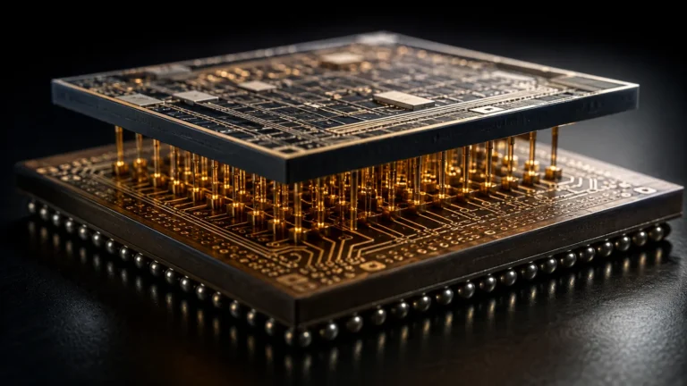
Solution: Startups like Ayar Labs developed optical I/O (Input/Output) chiplets. Instead of running copper traces to the edge of the server board, they placed a tiny silicon photonics chiplet directly next to the main processor on the same substrate.
Outcome: The processor hands its electrical data to the adjacent optical chiplet, which instantly converts it to light and fires it out of the server via fiber optics. This bypassed the traditional copper bottlenecks completely, allowing thousands of GPUs to synchronize their data seamlessly and train AI models in a fraction of the traditional time.
Lessons Learned: The limit to computational power is no longer how fast a chip can think; it is how fast a chip can talk. Optical networking at the chip level is the only physical path forward for AI scaling.
Future Outlook
Next 12–24 Months: The industry will see rapid adoption of Co-Packaged Optics (CPO) in high-end data center switches. Instead of plugging optical modules into the front of a server, the optics will be soldered directly alongside the main networking chips, significantly reducing power consumption and latency.
Next 3–5 Years: Optical interconnects will become the standard architecture for enterprise AI supercomputers. A new protocol called Compute Express Link (CXL) will operate over optical connections, allowing full memory disaggregation across entire data center campuses.
Next 10 Years: Research will shift from purely moving data with light to actually processing data with light. Optical computing—using photons passing through microscopic physical mazes to perform complex matrix multiplication—will emerge from laboratories to handle specific, highly complex AI inference tasks at zero electrical cost.
Most Likely Scenario: Silicon photonics will entirely replace copper wiring for all data center communications longer than one meter. Standard electrical wiring will be relegated exclusively to the final, microscopic distances inside the processor core itself, while light handles all external logistics.
Key Takeaways
- Silicon photonics converts electrical data into light to bypass the speed limits of copper wiring.
- It solves the critical I/O bottleneck currently suffocating massive AI supercomputers.
- Mach-Zehnder modulators flicker continuous laser beams to create the optical ones and zeros.
- Wave-division multiplexing allows multiple data streams to travel simultaneously using different colors of light.
- Photonic Integrated Circuits (PICs) allow optical components to be mass-produced in standard silicon foundries.
- Moving data with light produces virtually no heat, saving data centers millions in cooling costs.
- The technology enables “resource disaggregation,” allowing memory and processors to be physically separated across a facility.
Glossary
Co-Packaged Optics (CPO): The manufacturing technique of placing optical communication chips directly on the same substrate as the main processor to minimize electrical travel distance.
I/O Bottleneck: A hardware limitation where a computer processor calculates data faster than the input/output cables can physically transport it.
Mach-Zehnder Modulator: A microscopic optical component that rapidly alters the phase of a light wave to encode digital data onto a laser beam.
Photodetector: A semiconductor device, often made of Germanium, that catches incoming light and converts it back into an electrical signal.
Photonic Integrated Circuit (PIC): A microchip that contains multiple optical components (waveguides, modulators, detectors) etched into a single piece of silicon.
Resource Disaggregation: The architectural separation of a computer’s processor, memory, and storage, connected via high-speed networks rather than sharing a single motherboard.
Wave-Division Multiplexing (WDM): An optical technique that transmits multiple separate data streams simultaneously by using different wavelengths (colors) of laser light.
Waveguide: A microscopic, glass-like channel etched into silicon that physically guides the light beam across the chip.
Frequently Asked Questions
Why can’t we just make copper wires faster? Physics. Pushing higher frequencies through copper causes signal loss, electromagnetic interference, and massive heat generation. Copper has simply reached its thermodynamic limit for high-speed, long-distance data transfer.
How does the light get inside the silicon chip? Silicon does not emit light well, so an external laser (usually made of Indium Phosphide) is physically bonded to the silicon chip. It acts as a continuous light bulb, and the silicon components modulate that light.
Does this make the computer run cooler? Yes. Transmitting electrical data requires power and generates heat. Sending photons through a waveguide generates almost no heat, allowing data centers to significantly reduce their air conditioning requirements.
Are silicon photonics fragile? The chips themselves are solid-state and highly durable. However, the physical connection point where the external glass fiber optic cable attaches to the microscopic silicon waveguide is extremely sensitive to physical stress and alignment errors.
Is this the same as a fiber optic internet connection? It relies on similar physics, but at a vastly smaller scale. Fiber optic internet is the glass cable running under your street. Silicon photonics is the microscopic machinery that creates and reads the light signals at the end of that cable.
Will this replace normal processors? No. Processors will still use standard silicon transistors (electricity) to perform math and logic. Silicon photonics is exclusively used to handle the communication of data into and out of those processors.
Why is it so difficult to manufacture? Standard semiconductor foundries are built entirely to manipulate electrical properties. Adding optical components requires new materials (like Germanium and Indium Phosphide), entirely new testing equipment, and atomic-level packaging precision.
How does this impact artificial intelligence? AI models require thousands of chips working in perfect synchronization. Silicon photonics allows these chips to share massive amounts of data instantly, slashing the time it takes to train a model from months down to weeks.
Sources
• Institute of Electrical and Electronics Engineers (IEEE): Advances in Silicon Photonics Packaging
• Optica (formerly OSA): Integrated Photonics for Data Center Interconnects
• Massachusetts Institute of Technology (MIT) Microphotonics Center: Optical Communications Architecture
• Open Compute Project (OCP): Co-Packaged Optics Specifications