Advertisement
)

At a Glance
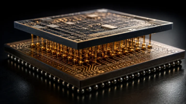
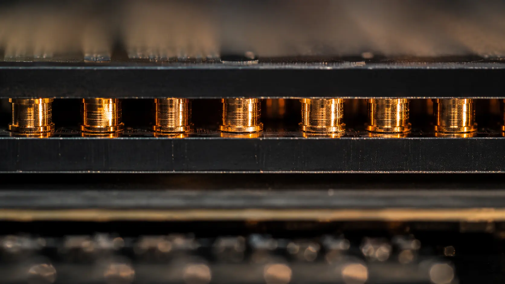
- Concept: Pressing two ultra-clean, perfectly flat silicon chips together so their dielectric (glass) surfaces bond like magnets, and then baking them so their internal copper wires expand and fuse into a single solid connection.
- Why it matters: AI accelerators and GPUs are starved for data. They require thousands of microscopic wires connecting them to their memory chips. Traditional solder beads take up too much physical space and melt if packed too tightly. Hybrid bonding shrinks the connection pitch below 10 µm, effectively removing the “speed limit” on data transfer.
- Who uses it: Tier-1 foundries like TSMC (SoIC platform) and Intel (Foveros Direct), massive memory suppliers (SK Hynix, Samsung, Micron) building High-Bandwidth Memory (HBM), and fabless giants (NVIDIA, AMD) designing AI superchips.
- Biggest takeaway: Hybrid bonding blurs the line between a printed circuit board and a microchip. By welding multiple different chiplets into one monolithic 3D block, engineers can mix and match components at will, driving down costs while delivering astronomical bandwidth.
In Simple Words
Inside your computer, the “brain” (the processor) and the “filing cabinet” (the memory) are separate chips. To talk to each other, they use microscopic metal wires.
Historically, we connected these chips by putting tiny beads of solder (meltable metal) between them and heating them up like a panini press. But as chips got faster and smaller, we needed thousands of more wires in the exact same space. If you put thousands of tiny solder beads too close together and melt them, they bleed into each other, creating a short circuit that instantly kills the computer.
Hybrid Bonding completely abandons the solder.
Instead of melting metal, engineers polish the surface of the two chips until they are smoother than a mirror. They expose them to a special plasma gas. When you press these two perfectly flat, clean chips together at room temperature, the molecules in the glass instantly grab each other and fuse solid without any glue. Then, the chips are placed in a gentle oven. The microscopic copper wires inside the glass expand from the heat, reach across the gap, and weld themselves together. The two chips effectively become one single, permanent piece of silicon.
Why This Matters
The global technology economy has hit the “Memory Wall.”
While the processing power of GPUs (like NVIDIA’s Blackwell or Hopper architectures) has scaled exponentially, the physical ability to pipe data in and out of those processors has struggled to keep pace. Generative AI models ingest terabytes of data per second. To feed this beast, memory chips must be stacked directly on top of or immediately adjacent to the logic chips.
Traditional 2.5D and 3D packaging relied on micro-bumps and thermocompression bonding (TCB). These legacy methods hit a physical brick wall at around a 20 µm pitch. Solder fundamentally cannot scale smaller.
Hybrid bonding shatters this ceiling, effortlessly scaling to sub-10 µm pitches (and driving toward 1 µm). By packing interconnects this tightly, hybrid bonding slashes interconnect electrical resistance by over 15%, brutally decreases power consumption, and provides a direct superhighway for AI data. The advanced packaging equipment market driving this shift—valued at roughly USD 1.8 billion in 2025—is projected to surge past USD 6 billion over the next decade. Without hybrid bonding, the AI hardware roadmap completely stalls.
The Big Picture
The integration of Hybrid Bonding represents a massive power shift in the semiconductor supply chain.
Historically, chip manufacturing was handled by highly advanced “Foundries” (like TSMC or Samsung), while the mundane task of wiring and boxing the chips was outsourced to “OSATs” (Outsourced Semiconductor Assembly and Test providers).
Because hybrid bonding requires ultra-clean environments, extreme chemical-mechanical precision, and nanoscale lithography alignments, the OSATs initially lacked the multi-billion-dollar cleanroom infrastructure to perform it. Consequently, front-end Foundries dragged the “packaging” process back in-house. TSMC’s System on Integrated Chips (SoIC) platform is a prime example, offering fabless companies a one-stop-shop that bypasses traditional OSATs. While OSATs (like Amkor and ASE) are now aggressively buying hybrid bonding tools to catch up, the technology permanently elevated “packaging” from an afterthought into the most critical step of semiconductor engineering.
How Hybrid Bonding Works
Fusing two solid materials without heat or adhesive requires manipulating atomic forces and thermodynamic expansion. Here is the first-principles breakdown.
1. The Fundamental Problem: The Limit of Solder
To increase bandwidth between two chips, you must increase the number of input/output (I/O) connections. If you use standard flip-chip solder micro-bumps, making them smaller and packing them closer together creates catastrophic issues. Solder is soft; when compressed, it squishes outward. If the pitch (distance between connections) drops below a certain threshold, the squishing solder bridges the gap to its neighbor, causing a fatal electrical short.
2. The Insufficiency of Thermocompression Bonding (TCB)
The industry tried to solve this using TCB, which uses heat and extreme pressure to fuse copper pillars with tiny solder caps. However, applying immense mechanical pressure to ultra-thin, delicate silicon chips causes them to buckle, warp, or crack, limiting yield rates and preventing the massive stacking of 8-high or 12-high memory modules.
3. The Core Mechanism: The Dual-Interface Bond
Hybrid bonding solves this by creating two distinct bonds simultaneously: a dielectric (glass-to-glass) bond and a metallic (copper-to-copper) bond, completely eliminating the solder interface.
4. Technical Depth: Plasma Activation and CMP Dishing
The process begins with Chemical-Mechanical Planarization (CMP). The chip surfaces are polished until they are completely flat. However, engineers intentionally polish the copper pads slightly deeper than the surrounding silicon dioxide (SiO_2) dielectric glass—a process known as “dishing.”
Next, a dual-plasma activation introduces hydroxyl (-OH) groups to the surface. When the two chips are pressed together at room temperature, the SiO_2 surfaces bond instantly via Van der Waals forces, locking the chips in perfect alignment. At this stage, the slightly recessed copper pads are not touching.
5. Real-World Consequences: Thermal Annealing and CTE
The bonded chips are then placed in an oven for “annealing” (typically between 150°C and 400°C). Here, the physics of the Coefficient of Thermal Expansion (CTE) take over. Copper expands at a much faster rate than the surrounding SiO_2 glass. As the chip heats up, the recessed copper pads expand outward, close the microscopic gap, and physically press into each other. Surface diffusion and grain boundary diffusion take over, fusing the copper grains into a single, void-free, highly conductive metallic joint. The result is a seamless 3D chip with thousands of invisible, perfectly insulated atomic wires.
Real-World Applications
Hybrid bonding has already exited the laboratory and is the foundational bedrock of tier-1 consumer and enterprise hardware.
CMOS Image Sensors (CIS): The earliest and most mature adoption of hybrid bonding was driven by Sony for smartphone cameras. By stacking the pixel sensor die directly on top of the image processing logic die, smartphones achieve incredibly fast autofocus, high frame-rate video, and superior low-light performance without expanding the physical size of the camera bump.
High-Bandwidth Memory (HBM): As the AI boom accelerates, suppliers like SK Hynix, Micron, and Samsung are utilizing hybrid bonding for next-generation HBM (HBM3E, HBM4). By eliminating the physical gap created by solder bumps, engineers drastically reduce the thermal resistance of the memory stack, allowing heat to escape faster and letting the memory run at significantly higher clock speeds.
Advanced 3D Logic (Chiplets): AMD’s 3D V-Cache technology stacks a massive slab of L3 cache memory directly on top of their CPU processing cores. By using TSMC’s hybrid bonding to fuse the cache directly to the logic, the processor retrieves data almost instantaneously, resulting in massive performance gains for high-end gaming and server-grade cloud compute.
Economic & Strategic Impact
The mass adoption of Die-to-Wafer (D2W) and Wafer-to-Wafer (W2W) hybrid bonding tools drastically alters the capital expenditure (CapEx) profile of semiconductor fabrication.
Building a hybrid bonding line requires ultra-precise cleanrooms, multi-chamber plasma activation systems, and sub-micron alignment metrology equipment. In 2026, over 38% of new hybrid bonding tool orders were directly driven by AI chip demand, a figure slated to surpass 50% by 2028.
This creates a high barrier to entry. Fabless chip designers (startups building custom AI accelerators) cannot afford to build this infrastructure. They are entirely reliant on the foundry-OSAT partnerships. Consequently, TSMC, Samsung Foundry, and Intel hold unparalleled pricing power in the advanced packaging market, transforming what was once the cheapest part of the chip-making process into a premium, high-margin revenue stream.
Advantages
- Sub-Micron Density: Achieves interconnect pitches below 10 µm, drastically increasing the number of I/O connections per square millimeter.
- Superior Thermal Pathways: Eliminating the underfill and solder gaps between chips removes insulating thermal barriers, allowing high-power logic and memory chips to cool efficiently.
- Lower Signal Latency: The direct copper-to-copper fusion creates shorter electrical paths, cutting resistance by roughly 15% and ensuring cleaner, faster signal integrity.
- Reduced Package Height: Eliminating the solder bumps allows chips to sit flush against one another, enabling 12-high and 16-high memory stacks to fit into ultra-thin mobile and server form factors.
Limitations
- Extreme Sensitivity to Contamination: Because the bonding relies on Van der Waals forces at the molecular level, a single microscopic speck of dust on the wafer will cause a massive, un-bonded “void bubble” that ruins multiple chips.
- CMP Topography Management: If the CMP “dishing” process leaves the copper too high, the chips will not sit flush, preventing the glass from bonding. If the copper is too deep, the thermal expansion will not bridge the gap, resulting in a dead electrical connection.
- Cost and Complexity: The tooling, plasma chambers, and alignment machinery are astronomically expensive, restricting top-tier hybrid bonding primarily to high-margin AI, server, and premium mobile components.
Common Misconceptions
Misconception: Hybrid bonding melts the copper to weld the chips together.
Reality: Copper melts at roughly 1,085°C—a temperature that would instantly incinerate a microchip. Hybrid bonding relies on solid-state diffusion at low temperatures (150°C to 400°C). The copper expands and the metallic grains merge together physically, but the metal never turns into a liquid.
Misconception: Any chip can be hybrid bonded to another chip.
Reality: To ensure the thousands of microscopic copper pads align perfectly, the two chips must be explicitly co-designed and mapped with flawless geometric precision. You cannot simply grab two random, pre-existing chips and press them together.
Misconception: OSATs are irrelevant now that foundries do packaging.
Reality: While foundries (like TSMC) lead the high-end Wafer-to-Wafer (W2W) sector, major OSATs (like Amkor and ASE) are spending billions to capture the Die-to-Wafer (D2W) market, which is critical for mixing and matching heterogeneous chiplets from different manufacturers.
What Most People Miss
The transition toward Polymer-Based Dielectrics.
Currently, the industry relies on rigid silicon dioxide (SiO_2) or silicon carbon nitride (SiCN) as the dielectric bonding surface. However, the Coefficient of Thermal Expansion (CTE) mismatch between solid copper and rigid glass creates immense stress during the annealing phase. In extremely large TSV (Through-Silicon Via) structures, this expanding copper can literally crack the surrounding glass.
To mitigate this, next-generation R&D is pushing toward compliant, organic polymer dielectrics (such as BCB or polyimide). These advanced polymers have a slight “give” to them. They can absorb the brutal stress of the expanding copper without fracturing, paving the way for larger, more robust high-power chiplet architectures in the late 2020s.
Comparison Table
| Feature | Flip-Chip Bumping (Solder) | Thermocompression Bonding (TCB) | Copper-to-Copper Hybrid Bonding |
| Minimum Pitch Limit | ~40 µm | ~20 µm | Sub-10 µm (Scalable to <1 µm) |
| Connection Medium | Tin/Lead Solder | Solder cap + Copper pillar | Direct Solid Copper Fusion |
| Operating Heat/Stress | High (Melts solder) | Extreme (Heat + physical pressure) | Low (Room temp bond + gentle anneal) |
| Dielectric Gap | Filled with epoxy resin | Filled with epoxy/underfill | No gap; directly fused glass |
| Primary AI Use Case | Legacy standard logic | Standard HBM and 2.5D packages | HBM4, 3D V-Cache, Next-Gen SoIC |
Case Study
Situation: As hyperscalers demanded exponentially larger Large Language Models (LLMs), NVIDIA and AMD required a way to exponentially increase the memory bandwidth of their AI accelerators. Traditional 2.5D packaging, which placed the memory next to the logic chip on a silicon interposer, was reaching its physical limits.
Challenge: The required solution was 3D packaging—stacking the logic and memory vertically. However, traditional micro-bumping took up too much physical headroom and introduced severe electrical and thermal resistance. If stacked using solder, the AI chips would overheat and throttle instantly.
Solution (TSMC SoIC Deployment): Fabless designers pivoted to TSMC’s System on Integrated Chips (SoIC) platform. TSMC utilized ultra-precise Die-to-Wafer (D2W) copper-to-copper hybrid bonding. They activated the dielectric surfaces with dual-plasma technology and bonded the chiplets at room temperature, subsequently annealing them to lock in the direct copper pathways.
Outcome: By 2025 and 2026, TSMC’s SoIC capacity utilization surged. The hybrid bonding technique effectively eradicated the solder gap. The direct copper-to-copper fusion dropped interconnect resistance by roughly 15%, significantly improved the thermal dissipation pathway, and allowed the AI accelerators to handle massive parallel processing workloads without melting.
Lessons Learned: The deployment cemented hybrid bonding as the undisputed king of 3D integration. It proved that achieving next-generation processing power was no longer just about shrinking transistors (Moore’s Law), but about mastering the thermodynamic geometry of advanced packaging.
Future Outlook
Next 12–24 Months
The explosion of Die-to-Wafer (D2W) capacity. As of early 2026, D2W is accounting for over 52% of new tooling orders. Because D2W allows a known-good die to be bonded to a wafer, it drastically improves yield rates over Wafer-to-Wafer (W2W) bonding (which inherently fuses some bad chips together). Foundries and OSATs will aggressively scale their D2W lines to meet the insatiable demand for custom, heterogeneous AI chiplets mixed from different process nodes.
Next 3–5 Years
The scaling of HBM4 and Monolithic Memory Integration. The next generation of High-Bandwidth Memory (HBM4) will completely discard traditional micro-bumps in favor of direct hybrid bonding for the memory stack. This will permit 16-high (and eventually 24-high) memory dies to fit inside the exact same Z-height restrictions as older generations, doubling total memory capacity without altering the physical chassis of the server blade.
Next 10 Years
The maturation of Sub-Micron Pitch Scaling and Optical Interconnects. As copper interconnect pitches shrink below 1 µm, the industry will eventually integrate silicon photonics directly into the hybrid bonded stack. We will witness chips that fuse copper for localized electrical power, while simultaneously aligning perfectly polished glass waveguides to shoot laser data directly between logic blocks, entirely rewriting the architecture of data center computing.
Most Likely Scenario
Hybrid bonding is not a transitional stepping stone; it is the permanent baseline architecture for the post-Moore’s Law era. The companies that successfully secure the billions of dollars in CapEx required to run pristine hybrid bonding fabrication lines—specifically TSMC, Intel, and Samsung—will hold absolute leverage over the global AI supply chain, while legacy bumping technology is permanently relegated to cheap, low-end consumer electronics.
Key Takeaways
- Hybrid bonding eliminates traditional solder bumps, replacing them with a dual-interface bond: a dielectric (glass) bond and a direct metallic (copper) bond.
- By pressing plasma-activated, perfectly flat chips together at room temperature, Van der Waals forces and covalent bonds fuse the glass surfaces instantly.
- A subsequent low-temperature annealing process (150°C to 400°C) forces the recessed copper pads to expand and weld together, creating a flawless electrical connection.
- The technology crushes interconnect pitches below 10 µm, unlocking the astronomical input/output (I/O) density required for modern AI accelerators and high-bandwidth memory (HBM).
- The hybrid bonding equipment market is projected to scale at a roughly 15% CAGR through 2034, signaling a massive shift in capital expenditure toward advanced packaging tools.
- Mastering the microscopic topography of Chemical-Mechanical Planarization (CMP) “dishing” is the critical manufacturing bottleneck preventing widespread OSAT adoption.
Glossary
Chemical-Mechanical Planarization (CMP): A critical manufacturing step using chemical slurries and physical polishing pads to smooth a silicon wafer until it is perfectly, microscopically flat.
Coefficient of Thermal Expansion (CTE): The rate at which a material expands when heated. Hybrid bonding relies on the fact that copper expands faster than surrounding glass to close the gap between chips.
Die-to-Wafer (D2W) Bonding: The process of taking individual, pre-tested chips (dies) and hybrid bonding them onto a larger, complete wafer. Favored for heterogeneous chiplet integration.
Dishing: A targeted CMP defect where the soft copper pads are polished slightly deeper than the harder surrounding glass, leaving a necessary microscopic recession for thermal expansion.
System on Integrated Chips (SoIC): TSMC’s proprietary, industry-leading advanced packaging platform that utilizes hybrid bonding for dense 3D chiplet stacking.
Thermocompression Bonding (TCB): A legacy advanced packaging technique that uses extreme heat and physical pressure to fuse tiny solder-capped copper pillars.
Van der Waals Forces: Weak, short-range atomic forces that pull molecules together. Used in the initial room-temperature stage of hybrid bonding to stick the glass surfaces together like a magnet.
Frequently Asked Questions
Why did we stop using solder for the most advanced chips?
Solder is soft and melts. When you try to put thousands of tiny solder connections into a space the size of a fingernail, the heat and pressure cause the solder beads to squish outward and touch each other, creating an electrical short that destroys the chip.
Does hybrid bonding require more energy than older methods?
Actually, it requires less. Traditional methods need extreme temperatures to melt metal or high mechanical pressure. Hybrid bonding starts with a room-temperature chemical reaction and requires a relatively gentle bake (anneal) to fuse the copper, reducing the thermal stress on the delicate silicon.
If the chips are glued together by glass, how does the electricity flow?
The copper wires are embedded inside the glass. When the chips are baked, the copper expands out of the glass and presses into the copper wire on the opposite chip. The metal physically merges, allowing electricity to flow perfectly while the surrounding glass provides insulation.
Who makes the machines that do this?
The advanced packaging equipment market is highly specialized. Companies like BESI (Besi Semiconductor Industries), Applied Materials, EV Group (EVG), and SUSS MicroTec dominate the manufacturing of these ultra-precise placement, plasma activation, and bonding tools.
Is this only used for AI chips?
While AI is driving the massive growth today, hybrid bonding was actually pioneered for consumer electronics. Sony used it years ago to stack smartphone camera sensors, allowing them to shrink the camera module while drastically improving image processing speed.
Sources
- Strategic Market Research: Hybrid Bonding Technology Market 2026: Expert-Crafted Insights You Can Trust
- Dataintelo: Hybrid Bonding Tool For Advanced Packaging Market Research Report 2034
- Intel Market Research: Hybrid Bonding Technology Market 2026 to 2034
- Patsnap Resource Center: Hybrid bonding in 3D IC packaging: Cu-to-Cu explained
- Semiconductor Engineering: Alternative Materials For Hybrid Bonding