Advertisement
)

At a Glance
- Concept: Utilizing silicon photonics to execute the core mathematics of neural networks—specifically matrix-vector multiplication—using intersecting beams of light.
- Why it matters: By early 2026, the global installed base of dedicated AI GPU servers was estimated to exceed 12 million units. These units consume over 150 terawatt-hours of electricity annually, a figure doubling nearly every two years. We have reached the thermal and power limits of traditional electronic processors.
- Who uses it: Leading startups like Lightmatter, Ayar Labs, Neurophos, and major semiconductor conglomerates like Marvell (following its acquisition of Celestial AI).
- Biggest takeaway: Photonic TPUs offer a massive leap in efficiency, with target energy consumption at the sub-picojoule level per operation. Startups have demonstrated systems achieving 100 teraoperations per second (TOPS) at under 15 watts, yielding a performance-per-watt ratio approximately 25 times superior to leading electronic GPU baselines.
In Simple Words
Inside a traditional computer chip, information is carried by electrons. To do math, the chip pushes these electrons through microscopic copper wires and billions of tiny switches (transistors). Pushing electrons through physical matter creates friction, which creates heat. When you scale this up to run massive Artificial Intelligence models, the chips get so hot they require thousands of gallons of water and massive air conditioners just to prevent them from melting.
Photonic TPUs solve this by replacing the electrons with photons (light).
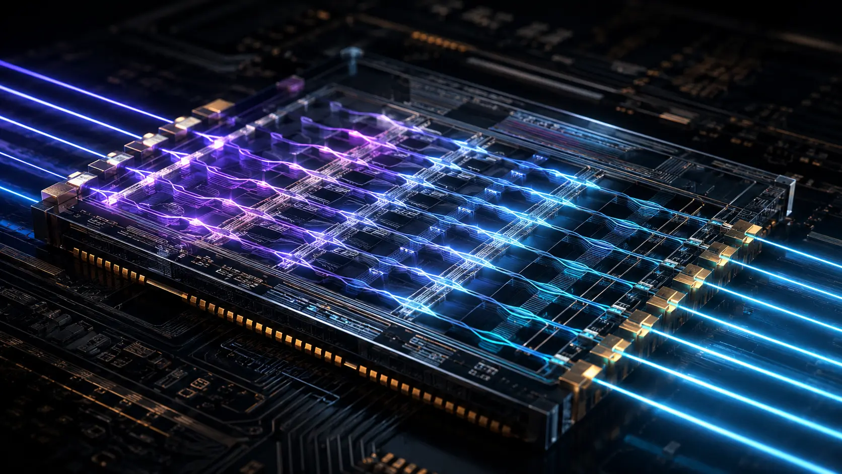
Instead of pushing electricity through copper, a Photonic TPU shines microscopic lasers through a maze of tiny silicon channels and prisms. When two beams of light cross paths, they perfectly pass through each other without causing friction or heat. By carefully designing the angles of this maze, the physical interference of the light waves naturally calculates the math required for AI. The answer pops out the other side at the literal speed of light. Because there are no moving electrons, the chip computes answers exponentially faster while staying cool, breaking the physical bottleneck holding back the next generation of supercomputing.
Why This Matters
The semiconductor industry is currently trapped in an unsustainable arms race.
To meet the insatiable demand for generative AI and Large Language Models (LLMs), chip designers have only one blunt solution: build bigger electronic chips. Processor die area is growing 13 to 18 percent annually. However, increasing the physical size of an electronic chip drastically increases the distance electrons must travel, causing capacitance and inductance delays that ruin performance.
Photonic AI accelerators bypass these constraints by transmitting data at the speed of light, producing near-zero crosstalk and minimal heat. The global market is transitioning rapidly, scaling from USD 1.8 billion in 2025 to a projected USD 14.6 billion by 2034. With pilot systems shipping to Tier-1 cloud customers in 2025 and 2026, mastering optical compute is the definitive requirement for any cloud provider aiming to dominate the datacenter infrastructure of the 2030s.
The Big Picture
The integration of light into computing is happening in distinct, strategic phases.
Before we can compute with light, we must connect with light. Companies like Lightmatter are tackling the interconnect crisis first. Their “Passage” platform utilizes 3D-integrated photonic circuits to deliver up to 114 Tbps of bandwidth, allowing massive GPU clusters to scale beyond the limits of copper electrical wires.
Once the data is flowing via optical interconnects, the next evolution is computation itself. By 2025, commercial validation arrived as devices like Lightmatter’s Envise demonstrated matrix multiplication using light, supported by publications in Nature. The ultimate 2030+ roadmap envisions a complete photonic stack, integrating lasers, optical interconnects, and photonic compute cores into a unified, wafer-scale datacenter fabric.
How Photonic TPUs Work
Replacing billions of transistors with optical pathways requires manipulating the wave-particle duality of light. Here is the first-principles breakdown.
1. The Fundamental Problem: Matrix Multiplication
Neural network inference relies overwhelmingly on one specific mathematical task: General Matrix-to-Matrix Multiplication (GEMM). In an electronic GPU, completing this math requires routing electrons through thousands of logic gates, consuming immense power and taking thousands of clock cycles.
2. The Insufficiency of Electronic Scaling
As electronic transistors shrink toward the 1-nanometer scale, they suffer from quantum tunneling (electrons leaking where they shouldn’t) and crippling heat density. Electronic chips simply cannot move data fast enough (the I/O bottleneck) or do the math cool enough to sustain exponential AI growth.
3. The Core Mechanism: Mach-Zehnder Interferometers (MZIs)
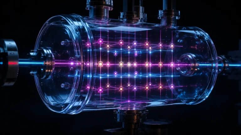
Photonic TPUs compute math natively using the physics of light. The core component is the Mach-Zehnder Interferometer (MZI). A laser beam enters the chip and is split into two separate paths. By applying a tiny voltage, the chip alters the phase of the light in one path. When the two paths are recombined, the light waves interfere with each other (amplifying or canceling each other out). The resulting light intensity represents the mathematical answer. By linking a massive mesh of these MZIs, the chip executes millions of calculations in a single sub-nanosecond optical pass.
4. Technical Depth: Wavelength Division Multiplexing (WDM)
Photons possess a unique property that electrons lack: multiple wavelengths (colors) of light can travel down the exact same physical fiber simultaneously without interfering with each other. Using Wavelength Division Multiplexing, a single waveguide can carry dozens of distinct data streams simultaneously. This grants photonic processors terahertz-range bandwidth, shattering the gigahertz-range ceilings of electronic processors.
5. Real-World Consequences: Hybrid Architectures
While light is flawless for linear matrix multiplication, it cannot natively handle the non-linear “activation functions” (like ReLU or Sigmoid) required for a complete neural network. Therefore, modern Photonic TPUs are hybrid architectures. They use a high-speed optical core to process the heavy matrix math, and then briefly convert the signal back to electrons so a small electronic unit can compute the non-linear activation. This hybrid design captures the extreme speed of light while maintaining mathematical completeness.
Real-World Applications of Photonic AI Accelerators
The leap from academic laboratories to enterprise hardware is already executing across several critical sectors.
Hyperscale Cloud Data Centers: Cloud providers are deploying 3D-integrated photonic interconnects to weave isolated servers into singular supercomputers. Lightmatter’s Passage platform enables edgeless I/O, allowing data to flow directly between chips optically, breaking the traditional “shoreline” bottlenecks that restrict how tightly GPUs can be packed together.
Distributed Edge AI: In environments where battery life and cooling are severely constrained—such as autonomous vehicles, medical imaging systems, and remote drone swarms—photonic solutions offer unparalleled Size, Weight, and Power (SWaP) advantages. Operating inference models at under 15 watts allows heavy AI workloads to run locally without connecting to the cloud.
Robot AI Brains: Robotics companies are evaluating photonic inference accelerators as a foundational compute layer for autonomous navigation. Because photonic chips offer sub-nanosecond latency (a single optical pass), robots can process computer vision and sensor data exponentially faster, drastically improving real-time reaction speeds in dynamic environments.
Economic & Strategic Impact
The transition to optical computing is re-wiring the global semiconductor supply chain.
Major photonic chip companies are predominantly headquartered in the United States. They benefit heavily from proximity to elite national laboratory infrastructure and DARPA-funded acceleration programs. Furthermore, federal initiatives like the CHIPS and Science Act allocated over USD 52 billion toward domestic semiconductor manufacturing, explicitly earmarking funds for advanced photonics research.
This concentration of R&D is drawing massive corporate capital. Marvell’s USD 3.25 billion acquisition of Celestial AI in December 2025 signaled that legacy electronic chipmakers view photonics as an existential necessity, rather than a fringe science. As startups partner with mega-foundries like GlobalFoundries and Amkor Technology to establish high-volume manufacturing, the industry is aggressively moving to secure the intellectual property surrounding silicon photonics packaging.
Advantages
- Sub-Nanosecond Latency: Matrix calculations are executed instantly as the light passes through the chip, entirely bypassing the thousands of clock cycles required by traditional silicon logic gates.
- Thermal Supremacy: Because photons do not generate resistance-based heat, cooling requirements are drastically slashed, allowing hardware to be packed with extreme density.
- Unmatched Energy Efficiency: Target architectures aim for sub-picojoule energy costs per multiply-accumulate (MAC) operation. This is orders of magnitude lower than the 10 to 100 picojoules required by conventional GPUs.
Limitations
- The Hybrid Conversion Penalty: Converting the optical signal back into an electrical signal (O-E-O conversion) to perform non-linear activation functions introduces latency and power costs that threaten to diminish the overall efficiency of the processor.
- Laser Integration Challenges: Integrating hundreds of microscopic lasers (External Light Sources) onto a single silicon chip without them degrading over time is a massive manufacturing hurdle.
- Analog Precision Limits: Electronic digital chips deal in perfect 1s and 0s. Photonic chips rely on analog interference, meaning tiny manufacturing imperfections or thermal fluctuations in the silicon can introduce slight mathematical errors (noise) into the calculations.
Common Misconceptions
Misconception: Photonic chips use regular light bulbs to work.
Reality: These processors require highly specialized, coherent lasers. The light waves must be perfectly synchronized so that their phase shifts can be accurately measured when they interfere with one another.
Misconception: Optical processors will completely replace electronic CPUs and GPUs.
Reality: Photonic TPUs are highly specialized co-processors. They act as a hybrid accelerator for heavy linear math (matrix multiplication). A standard electronic CPU will still be required to run the operating system, orchestrate data movement, and handle non-linear logic.
Misconception: This technology is decades away from being usable.
Reality: The market has already transitioned from proof-of-concept into early commercial deployments. Top-tier cloud hyperscalers began integrating pilot photonic interconnects and accelerators into their datacenters throughout 2025 and 2026.
What Most People Miss
The quiet revolution of Co-Packaged Optics (CPO).
People assume you can just unplug an old GPU and plug in a Photonic TPU. In reality, the integration requires a physical redesign of the motherboard. The industry is rapidly advancing from “pluggable” optics to Co-Packaged Optics (slated for mass integration by 2027). CPO takes the optical transceivers and places them on the exact same substrate package as the electronic processor. This eliminates the final inches of copper wiring, slashing the electrical power required to move data from the laser to the chip, and serving as the absolute prerequisite for native photonic computing.
Electronic GPUs vs Photonic TPUs
| Feature | Electronic GPU / ASIC | Photonic TPU Accelerator |
| Matrix Multiply Latency | Microsecond to Millisecond | Sub-nanosecond (Single Optical Pass) |
| Energy per MAC Operation | 10 to 100 picojoules | Sub-picojoule target |
| Bandwidth Limits | Gigahertz-range | Terahertz-range |
| Heat Generation | Extremely High (Major bottleneck) | Very Low |
| Non-Linear Operations | Native to silicon | Requires hybrid electronic unit |
Case Study
Situation: As AI models scaled to trillions of parameters, hyperscale cloud providers faced a literal wall. The required clusters of GPUs generated too much heat, and moving data electrically between the thousands of chips caused unacceptable latency and power drain.
Challenge: The industry needed a compute engine that could execute massive matrix multiplications without triggering catastrophic thermal throttling or bottlenecking at the I/O interface.
Solution (The Lightmatter Envise Deployment): Lightmatter, an MIT spin-off that raised USD 850 million and hit a USD 4.4 billion valuation by 2024, deployed Envise—the world’s first photonic processor executing production AI workloads. Inside Envise, four photonic chips manipulated 512 light beams through over 200,000 optical components.
Outcome: By utilizing elegant physics, where the interference of light naturally computes linear transformations without moving electrons, Envise achieved unprecedented performance. Lightmatter demonstrated systems delivering 100 teraoperations per second (TOPS) at under 15 watts of power. The architecture proved that 25x performance-per-watt superiority over standard GPUs was physically achievable.
Lessons Learned: The success of Envise proved that solving the power crisis of AI requires stepping outside of traditional electrical engineering. By embracing silicon photonics, the industry validated that the future of computing scaling lies in mastering the fundamental properties of light.
Future Outlook
Next 12–24 Months
The era of the Photonic Interconnect. Through 2026 and 2027, the focus will remain heavily on solving the I/O bottleneck. Technologies like Near-Packaged Optics (NPO) and Co-Packaged Optics (CPO) will enter broad production deployments. We will see massive AI server racks bound together entirely by silicon photonics, allowing thousands of distinct GPUs to act seamlessly as a single, unified supercomputer with terabytes of frictionless bandwidth.
Next 3–5 Years
The mainstream deployment of Hybrid Optical Accelerators. As the manufacturing processes at foundries mature, the cost of printing Mach-Zehnder Interferometer meshes onto silicon will plummet. By 2028, hybrid Photonic TPUs will become standard specialized co-processors in Tier-1 data centers, specifically tasked with accelerating the linear layers of massive transformer models and convolutional neural networks.
Next 10 Years
The Holy Grail: The Full Photonic Stack. Looking toward 2030 and beyond, companies will aim to finalize the integration of computation, lasers, and interconnects into an active photonic interposer. The ultimate R&D goal is overcoming the hybrid conversion penalty. If researchers can commercialize advanced non-linear optical materials, we will witness the birth of 100 percent purely optical neural networks, where data enters as light, is calculated as light, and exits as light, culminating in an essentially heat-less, limitless artificial intelligence engine.
Most Likely Scenario
Photonic processing will not kill the traditional silicon industry; it will permanently integrate with it. The datacenter of the 2030s will be an intricately layered hybrid system. Standard electronics will continue to orchestrate memory and logic, while a dense, high-speed optical nervous system handles the heavy mathematical lifting and data transit, ensuring that the exponential growth of artificial intelligence does not collapse the global power grid.
Key Takeaways
- Photonic AI accelerator chips process matrix-vector multiplications using light signals instead of electrons, eliminating thermal generation and achieving speeds measured at the literal speed of light.
- The global market for these processors is expanding at a 26.3 percent CAGR, projected to reach USD 14.6 billion by 2034.
- The core compute mechanism relies on a mesh of Mach-Zehnder interferometers (MZIs), where the physical interference of intersecting laser beams naturally calculates the math required for AI.
- Current optical chips achieve sub-nanosecond latency and sub-picojoule energy costs per operation, vastly outperforming the microsecond delays of standard GPUs.
- Because light cannot natively perform non-linear activation functions, modern Photonic TPUs utilize a hybrid architecture, passing linear math to optical cores and non-linear math to electronic units.
- Startups like Lightmatter are leading the charge, building 3D-integrated photonic interconnects (Passage) and fully functional photonic compute accelerators (Envise) for next-generation datacenters.
Glossary
Co-Packaged Optics (CPO): An advanced integration technique that places optical transceivers directly next to the compute chip on the same substrate, drastically reducing electrical power consumption and signal delay.
GEMM (General Matrix-to-Matrix Multiplication): The foundational mathematical operation that underpins nearly all modern neural network inference and training.
Mach-Zehnder Interferometer (MZI): A microscopic optical device that splits a beam of light, alters the phase of one path, and recombines them. The resulting interference is used to perform arithmetic calculations optically.
O-E-O Conversion (Optical-Electrical-Optical): The process of translating a light signal into an electrical signal and back again. Minimizing this conversion is a primary goal in photonic processor design.
Photonic TPU: A Tensor Processing Unit designed to accelerate machine learning workloads by substituting standard electrical logic gates with optical components.
Wavelength Division Multiplexing (WDM): A technology that multiplexes a number of optical carrier signals onto a single optical fiber by using different wavelengths (colors) of laser light, vastly increasing data bandwidth.