Advertisement
)
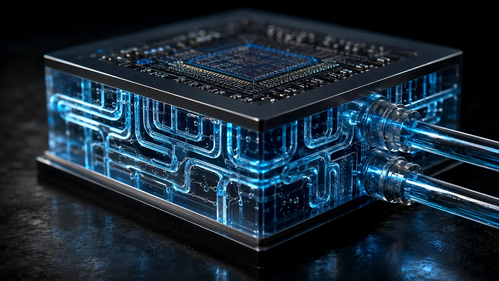

A modern artificial intelligence chip generates more heat per square centimeter than the nozzle of a commercial rocket engine. As the tech industry races to build multi-trillion-parameter AI models, companies are cramming hundreds of billions of transistors into microscopic spaces, increasingly stacking them like digital skyscrapers (3D Integrated Circuits). But this creates a catastrophic physics problem: the transistors in the middle of these stacks are effectively trapped in a thermal prison. They are boiling themselves alive.
Traditional air conditioning, and even liquid-cooled cold plates bolted to the top of the chip, are no longer sufficient. The heat simply cannot travel through the silicon layers fast enough to escape. To prevent the data centers of the late 2020s from suffering widespread thermal throttling, engineers have stopped trying to cool the outside of the chip. Instead, they are drilling directly into the silicon itself. By etching microscopic “blood vessels” into the structural foundation of the processor and pumping liquid coolant directly through its veins, the semiconductor industry is fundamentally redefining the anatomy of a computer chip.
What is Microfluidic In-Chip Cooling?
Microfluidic in-chip cooling is a thermal management architecture that etches microscopic liquid channels directly into the silicon substrate of a semiconductor. By pumping dielectric fluid or deionized water through these internal pathways, it removes heat directly at the transistor level, completely bypassing the thermal resistance of external heat sinks and interface pastes.
At a Glance
- Concept: Using Deep Reactive-Ion Etching (DRIE) to hollow out microscopic capillary networks inside the inactive layers of a silicon wafer, creating an artificial circulatory system for liquid coolant.
- Why it matters: AI accelerator chips have surpassed heat fluxes of 500 Watts per square centimeter (W/cm²). External cooling plates cannot absorb this heat fast enough. In-chip cooling slashes the distance heat must travel from millimeters to microns.
- Who uses it: Cutting-edge research consortiums (like imec), defense agencies (DARPA’s ICECool program), and major foundries (TSMC) exploring ultimate thermal solutions for 3D packaging.
- Biggest takeaway: This technology permanently merges semiconductor foundries with fluid dynamics. Chipmakers can no longer just design electrical circuits; they must now design highly pressurized plumbing systems on a nanometer scale.
In Simple Words
Think of a computer chip like a car engine.
In the early days of automobiles, engines were “air-cooled.” They had metal fins on the outside, and as the car drove, the wind cooled the metal. But as engines got bigger and produced more horsepower, air wasn’t enough. The engine would melt. So, engineers invented the radiator and the “water jacket”—they hollowed out channels inside the heavy metal engine block and pumped liquid coolant directly through the metal walls to pull the heat out from the inside.
The computer chip industry is making this exact same transition today.
For 50 years, we cooled computer chips by blowing fans across metal fins placed on top of them. But today’s AI chips generate so much horsepower that the top of the chip can’t pull the heat away fast enough from the bottom. Microfluidic In-Chip Cooling is the water jacket for the microchip. Scientists use lasers and acid to drill microscopic tunnels through the actual silicon of the chip itself. They pump fluid through these tunnels, carrying the heat away instantly before the chip can ever get hot.
Why This Matters
The end of Moore’s Law is not being dictated by the size of transistors, but by the “Thermal Wall.”
As we move into the era of 2-nanometer nodes and beyond, the density of transistors has outpaced our ability to cool them. In a standard 2D chip, hotspots can reach 500 to 1,000 W/cm². To solve memory bottlenecks, the industry is aggressively shifting to 3D packaging—stacking logic chips and High-Bandwidth Memory (HBM) directly on top of each other.
However, stacking chips is like stacking mattresses; the one on the bottom completely loses its ability to dissipate heat. If the bottom AI logic die hits 105°C, it will permanently damage the delicate memory chips stacked above it. Without microfluidic in-chip cooling, vertical 3D scaling is physically impossible. Mastering this technology is the absolute prerequisite for building the next decade of ultra-dense, low-latency AI supercomputers.
The Thermal Wall: Why AI Requires In-Chip Cooling
The evolution of data center cooling is a story of shrinking distances.
We moved from cooling the room (CRAC units), to cooling the server rack (rear-door heat exchangers), to cooling the top of the chip (Direct-to-Chip cold plates). Microfluidics represents the terminal stage of this evolution: bringing the coolant directly to the atomic heat source.
While massive hyperscale facilities in 2026 are heavily adopting single-phase and two-phase Immersion Cooling (submerging entire servers in vats of fluid), immersion is a blunt instrument. It requires completely redesigning the entire data center architecture. Microfluidic in-chip cooling is surgically precise. It attacks the thermal bottleneck at the silicon wafer level, allowing standard data center layouts to field massively overpowered chips without building liquid swimming pools for their servers.
How Microfluidic In-Chip Cooling Works (Mechanics)
Creating a high-pressure plumbing network inside a brittle crystal without destroying the electrical circuits requires atomic-level precision. Here is the first-principles breakdown.
1. The Fundamental Problem: The TIM Bottleneck
In traditional cooling, a liquid cold plate is bolted to the top of the chip. However, the surface of a chip and the surface of a cold plate are not perfectly flat; at a microscopic level, they look like jagged mountain ranges. To fill the air gaps, engineers use Thermal Interface Material (TIM)—a thermal paste. Unfortunately, TIM is an incredible bottleneck. It has high “thermal resistance,” acting like a heavy blanket that slows the heat from reaching the cold plate.
2. The Insufficiency of External Liquid Cooling
Even if you use ultra-expensive Liquid Metal TIMs, the heat still has to travel through the silicon substrate (the structural back of the chip) to reach the paste. Silicon is a semiconductor, but it is a relatively poor conductor of heat. By the time the heat fights its way through the silicon and the TIM, the transistors at the bottom have already overheated.
3. The Core Mechanism: Deep Reactive-Ion Etching (DRIE)
To eliminate the TIM and the silicon distance, foundries use Deep Reactive-Ion Etching (DRIE). During the manufacturing process, before the chip is packaged, the foundry etches thousands of microscopic trenches (often 50 to 100 microns wide) directly into the inactive backside of the silicon wafer. A glass or silicon lid is then bonded over these trenches, sealing them into closed capillary tubes.
4. Technical Depth: Two-Phase Evaporative Cooling
Once sealed, dielectric fluid (or highly purified water) is pumped through the chip. The most advanced systems use Two-Phase Cooling. As the liquid passes directly over the blistering hot transistor junctions, it absorbs the heat and instantly boils, turning into a vapor. The physics of changing states from a liquid to a gas (latent heat of vaporization) absorbs an astronomical amount of thermal energy. The vapor rushes out of the chip, carries the heat to an external radiator where it condenses back into a liquid, and the cycle repeats.
5. Real-World Consequences: Near-Zero Thermal Resistance
By putting the boiling fluid just 20 to 50 microns away from the transistor, the thermal resistance of the system drops by nearly 10x compared to traditional cold plates. The TIM is completely eliminated. The chip can now dissipate localized heat fluxes exceeding 1,000 W/cm², unlocking the ability to stack multiple chips vertically without the bottom chip incinerating the stack.
Real-World Applications of 3D Microfluidic Cooling
While notoriously difficult to manufacture at scale, microfluidic cooling is breaking into high-stakes environments.
3D Integrated Circuits (High-Bandwidth Memory): The most pressing commercial application is 3D memory stacks. Next-generation High-Bandwidth Memory (like HBM4 and HBM5) requires stacking up to 16 silicon dies on top of a base logic die. Research consortiums like imec have successfully demonstrated microfluidic channels etched directly into the interposer (the silicon bridge connecting the chips), actively pumping coolant between the microscopic gaps of the memory stack to maintain the strict 85°C to 95°C operational limits.
Defense and Aerospace (DARPA ICECool): Military hardware operates under severe Size, Weight, and Power (SWaP) constraints. High-powered radar arrays and directed-energy weapons (lasers) generate massive thermal spikes in milliseconds. Through the ICECool (Intra/Interchip Enhanced Cooling) program, DARPA defense contractors successfully embedded microfluidics into Gallium Nitride (GaN) radio-frequency amplifiers, allowing military drones and fighter jets to field radar systems that are orders of magnitude more powerful without increasing the physical size of the cooling unit.
Automotive Power Electronics: Electric vehicles rely on Silicon Carbide (SiC) power inverters to push hundreds of kilowatts of energy from the battery to the wheels. EV manufacturers are actively prototyping microfluidic heat sinks bonded directly to the bare SiC dies, ensuring the chips do not melt during repeated ultra-fast 350kW DC charging sessions or heavy acceleration.
Economic & Strategic Impact
Integrating plumbing into the silicon die forces a violent disruption of the semiconductor supply chain.
Historically, thermal management was the responsibility of the Original Equipment Manufacturer (OEM) like Dell or HP; they bolted the heat sink on after buying the chip from NVIDIA or Intel. Microfluidic in-chip cooling shifts the economic burden and intellectual property of cooling entirely onto the foundries (TSMC, Samsung, Intel) and advanced packaging OSATs (Outsourced Semiconductor Assembly and Test).
If a fluidic channel clogs or leaks inside a $40,000 AI accelerator, the entire chip is destroyed. The foundry must guarantee the structural integrity of the micro-plumbing at the nanometer scale. This requires massive Capital Expenditure (CapEx) for new specialized fluidic testing equipment on the wafer fabrication line, temporarily driving up the cost of premium silicon but establishing a massive technological moat for the foundries capable of achieving high manufacturing yields.
Advantages
- Ultimate Heat Dissipation: Can comfortably manage heat fluxes above 500-1000 W/cm², a threshold where traditional air and external liquid cold plates fail completely.
- Enables True 3D Stacking: By routing coolant between layers of stacked silicon, it eliminates the thermal isolation of the bottom-tier chips, unlocking vertical Moore’s Law scaling.
- Zero TIM Degradation: Eliminates the use of Thermal Interface Materials (thermal paste), which naturally pump out, dry up, and degrade over a 5-year data center lifespan.
- Waste Heat Recovery: The high-temperature fluid exiting the chip is highly efficient for secondary use, allowing data centers to pipe 60°C+ water directly into municipal district heating systems for nearby homes and businesses.
Limitations
- Extreme Manufacturing Complexity: Etching deep channels into a silicon wafer creates severe mechanical stress, making the already fragile silicon die highly susceptible to cracking during the packaging process.
- Fouling and Clogging: Micro-channels are narrower than a human hair. Any microscopic debris, oxidation, or biological growth in the coolant loop will instantly clog the channel, triggering a localized thermal runaway that destroys the chip.
- High Pressure Drops: Forcing viscous liquid through microscopic tunnels requires immense pressure. The energy required to run the external pumps can sometimes offset the energy saved by the efficient cooling.
- Leakage Catastrophe: A micro-fracture that leaks highly conductive water or pressurized dielectric fluid directly into the 3D logic package results in the instant, catastrophic failure of a multi-tens-of-thousands-of-dollars asset.
Common Misconceptions
Misconception: This is the same as Direct-to-Chip (Cold Plate) liquid cooling.
Reality: Direct-to-Chip cooling places a metal block full of liquid on top of the finished chip package. Microfluidic In-Chip cooling etches the liquid channels directly into the bare silicon crystal inside the package itself.
Misconception: The liquid physically touches the electrical circuits.
Reality: The liquid does not touch the active transistors. The silicon wafer has an “active” side (where the microscopic circuits are printed) and a thick “inactive” structural backside. The microfluidic channels are etched into the inactive backside.
Misconception: Microfluidic cooling uses liquid nitrogen.
Reality: Cryogenic cooling is generally reserved for quantum computing. Microfluidic AI cooling typically uses highly purified deionized water (because water has an exceptionally high heat capacity) or engineered two-phase dielectric fluids (like 3M Novec alternatives) that boil at relatively low temperatures.
What Most People Miss
The physics of Two-Phase Latent Heat.
Most people assume liquid cooling works by pumping cold water in, letting it absorb heat until it gets warm, and pumping the warm water out (Single-Phase). While this works, it requires a massive volume of fluid moving very fast.
The true breakthrough of microfluidics is Two-Phase Boiling. Engineers specifically design the internal channels with microscopic textures that act as “nucleation sites” (like the rough spots in a pot of boiling water). When the fluid hits the hot spot above a transistor, it instantly flash-boils into vapor. Turning a liquid into a gas absorbs a staggering amount of energy (Latent Heat of Vaporization) without the temperature of the fluid itself increasing. This allows the chip to absorb incredibly dense thermal spikes using a tiny trickle of fluid, rather than a massive, high-pressure firehose.
Comparison Table
| Cooling Technology | Thermal Resistance | Max Heat Flux Capability | Primary Application | Risk of Coolant Leak to Silicon |
| Air Cooling (Heat Sink) | High | ~ 100 – 150 W/cm² | Standard CPUs / Consumer GPUs | Zero |
| Direct-to-Chip Cold Plate | Moderate (TIM Bottleneck) | ~ 300 – 500 W/cm² | H100 / Enterprise AI Clusters | Low (External to package) |
| Immersion Cooling | Low | ~ 200 – 300 W/cm² | High-Density Crypto/Cloud Racks | Moderate (Non-conductive fluid) |
| Microfluidic In-Chip | Ultra-Low (No TIM) | > 1,000 W/cm² | Next-Gen 3D Stacked AI / HBM | High (Internal to bare die) |
Case Study
Situation: As Moore’s Law slowed down in the 2D plane, the semiconductor industry pivoted to 3D heterogeneous integration—stacking Logic, Memory, and Power-delivery chips like a high-rise building. However, testing revealed a fatal flaw: the heat generated by the dense logic chips at the bottom of the stack had no physical escape route, causing the top-level memory chips to overheat and fail.
Challenge: Researchers needed a way to remove hundreds of watts of heat from the microscopic gaps between the stacked chips, completely bypassing the need to push the heat up through the roof of the package.
Solution (The imec 3D Microfluidic Test Vehicle): Researchers at imec (the world-leading nanoelectronics R&D hub in Belgium) developed a monolithic microfluidic interposer. Instead of trying to cool the top of the stack, they etched 50-micron-wide cooling channels directly into the silicon interposer—the foundational base layer that the 3D chips sit on. They utilized a specialized 3D-printed manifold to route pressurized coolant directly into these micro-capillaries.
Outcome: The results fundamentally altered 3D packaging physics. By running fluid directly under the heat sources, imec achieved a staggering reduction in thermal resistance. They demonstrated the ability to cool heat fluxes exceeding 600 W/cm² while maintaining chip temperatures well below the 85°C critical threshold, all without a bulky external cold plate.
Lessons Learned: The imec test vehicle proved that 3D scaling is a fluid dynamics problem, not just an electrical one. By treating the silicon interposer as a highly complex liquid manifold, the industry realized that the ultimate solution to the thermal wall is co-designing the electrical circuits and the fluidic cooling channels simultaneously from day one of the chip’s architecture.
Future Outlook
Next 12–24 Months
The bridge phase: Direct-to-Silicon Cold Plates. Before foundries risk etching channels directly into the silicon die, the industry is transitioning to lidless packages. AI chipmakers are removing the metal Integrated Heat Spreader (IHS) and applying the microfluidic cold plate directly against the bare silicon die, utilizing highly advanced Liquid Metal TIMs. This drastically reduces thermal resistance and serves as the immediate 2026/2027 stopgap for 1,000-watt+ AI accelerators.
Next 3–5 Years
The commercialization of the Fluidic Interposer. By the end of the decade, advanced packaging facilities (like TSMC’s CoWoS lines) will introduce active silicon interposers with pre-etched microfluidic cooling channels. High-performance computing customers will purchase AI chips that have standardized micro-plumbing inlet/outlet ports built directly into the silicon substrate, requiring server manufacturers to develop ultra-precise, blind-mate liquid connectors at the motherboard level.
Next 10 Years
The Monolithic 3D Electro-Fluidic Chip. By the mid-2030s, the boundary between the cooling system and the transistor will vanish. Foundries will utilize advanced nanoscale 3D printing and atomic layer deposition to weave microscopic cooling capillaries directly through the active layers of the transistor stacks, mimicking the capillary blood vessels of the human brain. This true monolithic integration will yield chips capable of localized heat fluxes approaching 2,000 W/cm², unlocking the physical architectures required for Artificial General Intelligence (AGI).
Most Likely Scenario
Microfluidic in-chip cooling will remain a highly bespoke, premium technology reserved exclusively for top-tier AI training accelerators, military radar, and high-frequency trading ASICs. The extreme cost and yield risks associated with etching silicon plumbing mean that standard commercial servers and consumer electronics will continue to rely on traditional external cold plates and vapor chambers for the foreseeable future.
Key Takeaways
- Microfluidic in-chip cooling etches microscopic liquid channels directly into the inactive silicon backside of a computer chip to remove heat at the source.
- By bringing the liquid coolant just microns away from the transistors, it completely eliminates the thermal resistance caused by thermal paste (TIM) and heavy metal heat spreaders.
- The technology is an absolute physical prerequisite for future 3D Integrated Circuits, allowing coolant to flow between stacked chips to prevent the bottom layers from incinerating the top layers.
- Advanced systems use two-phase cooling, where the fluid absorbs the heat and flash-boils into a vapor, utilizing the latent heat of vaporization to absorb massive thermal spikes.
- The primary commercial bottleneck is the catastrophic risk of a microscopic clog or fluid leak inside a premium, multi-tens-of-thousands-of-dollars AI accelerator during operation.
- This technology forces a massive supply chain shift, moving the responsibility for cooling away from server manufacturers (like Dell) and directly into the hands of semiconductor foundries (like TSMC).
Glossary
3D IC (Three-Dimensional Integrated Circuit): A microchip manufactured by stacking silicon wafers or dies vertically and connecting them using through-silicon vias (TSVs) to act as a single device.
Deep Reactive-Ion Etching (DRIE): A highly precise manufacturing process that uses chemically reactive plasma to excavate deep, steep-sided holes and trenches into silicon wafers.
Dielectric Fluid: A non-conductive liquid used as a coolant. If it leaks onto active electronics, it will not cause a short circuit (unlike water).
Heat Flux (W/cm²): The amount of heat transferred per unit area. Modern AI chips have massive heat flux, meaning a terrifying amount of heat is concentrated in a tiny physical space.
Latent Heat of Vaporization: The massive amount of physical energy required to change a substance from a liquid to a gas (e.g., boiling water) without changing its temperature.
Thermal Interface Material (TIM): A paste or pad used to fill the microscopic air gaps between a computer chip and a heat sink to improve heat transfer. It acts as a major bottleneck in traditional cooling.
Frequently Asked Questions
Will water leak inside the computer chip and destroy it?
Leakage is the primary risk of microfluidics. To mitigate this, many advanced systems use dielectric fluids (engineered liquids that do not conduct electricity). If a micro-fracture occurs and dielectric fluid leaks onto the circuits, it will not cause a short circuit, though it may still ruin the localized cooling pressure.
Why can’t we just use bigger fans?
Air is a terrible conductor of heat. AI chips have crossed a thermal density threshold where even hurricane-force air blown across a massive metal heatsink simply cannot absorb and carry the heat away fast enough before the chip hits its 105°C thermal limit and shuts down.
Is this technology already being used in my laptop?
No. Laptops and standard consumer PCs use “heat pipes” or “vapor chambers,” which are sealed metal tubes that contain a tiny bit of fluid. Microfluidic in-chip cooling is an active, pressurized plumbing system etched into the bare silicon itself, reserved only for multi-million-dollar AI supercomputers and defense tech.
How do they connect the tiny hoses to the silicon chip?
This is a massive engineering challenge. Engineers use specialized micro-manifolds (often 3D printed from high-grade polymers or ceramics) that bond to the inlet/outlet ports on the silicon. These manifolds act as physical adapters, stepping up the microscopic silicon channels to standard millimeters-wide server hoses.
Does microfluidic cooling consume a lot of electricity?
Yes. Pushing viscous liquid through microscopic capillaries requires powerful, high-pressure mechanical pumps. The energy required to run these external pumps (pumping power) is a significant factor that must be weighed against the energy saved by cooling the chip efficiently.
Sources
[1] imec: 3D integration and microfluidic cooling for high-performance computing (2025/2026 Research Briefs)
[2] Defense Advanced Research Projects Agency (DARPA): Intra/Interchip Enhanced Cooling (ICECool) Program Outcomes
[3] IEEE Transactions on Components, Packaging and Manufacturing Technology: Two-Phase Microfluidic Cooling of 3D-ICs
[4] TSMC: Advanced Packaging and Thermal Management Solutions for 3D Fabric (Symposium Data 2025)
[5] Semiconductor Engineering: The Shift to In-Chip Cooling for AI Accelerators