Advertisement
)
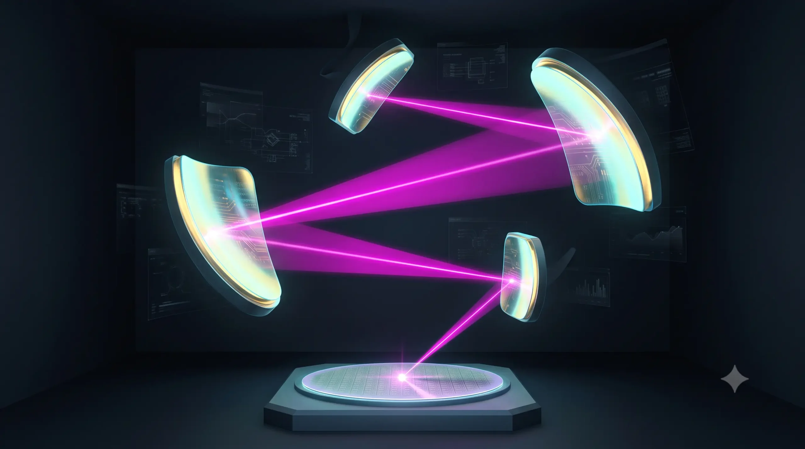

If you open up a modern smartphone or an AI server, you are looking at an object that defies standard physics. The transistors inside those microchips are now smaller than a virus. They are so microscopic that we have physically run out of room on the silicon wafer. To make artificial intelligence smarter, we have to pack even more transistors into the exact same amount of space. But there is a massive problem: the “brush” we use to paint these circuits is light, and the light is getting too “fat.”
For the past few years, the semiconductor industry has used Extreme Ultraviolet (EUV) light to print circuits. But to hit the sub-2nm milestone required for the next decade of computing, standard EUV light is no longer sharp enough. The lines blur together. To fix this, scientists didn’t change the light—they changed the mirrors. They built the most complex, expensive machine in human history: a $350 million, bus-sized apparatus that catches light, stretches it like a funhouse mirror, and focuses it down to a near-atomic point. Why should you care right now? Because whoever controls these mirrors controls the entire future of the global economy. This is High-NA EUV lithography, the multi-hundred-million-dollar gamble that will determine whether the artificial intelligence revolution continues, or stalls out entirely.
What is High-NA EUV Lithography?
High-NA EUV lithography is an advanced semiconductor manufacturing technology that increases a lithography machine’s Numerical Aperture (NA) from 0.33 to 0.55. By utilizing larger, specialized mirrors to focus extreme ultraviolet light more sharply, it enables the precise printing of sub-2nm transistors required for next-generation microchips.
At a Glance
- Concept: Building a bigger “lens” (Numerical Aperture) to focus light more tightly, allowing manufacturers to draw thinner lines on silicon wafers without the ink blurring.
- Why it matters: Standard EUV machines max out around the 3nm node. To go smaller, factories have to “double-print” (multi-patterning), which is expensive and slow. High-NA allows them to print sub-2nm lines in a single, fast pass.
- Who uses it: Intel is the aggressive first-mover, utilizing it for their Intel 14A node. TSMC and Samsung are evaluating adoption timelines for the late 2020s. ASML is the sole company on Earth capable of building the machine.
- Biggest takeaway: Because the mirrors had to be designed differently (anamorphic optics), the machine can only print half as much chip surface area at a time. This forces the physical robotic stages holding the wafers to move at terrifyingly fast speeds to keep up with production quotas.
In Simple Words
Making a microchip is like using a flashlight and a stencil to project a shadow onto a piece of photographic paper. The lines on the stencil become the wires of the microchip.
To make the wires smaller, you need a sharper shadow.
In traditional EUV Lithography, we use invisible, high-energy light with a wavelength of 13.5 nanometers. But as the wires on the stencil get closer and closer together, the light starts to bend around the edges, making the shadow blurry.
To fix the blur, you need a bigger lens to catch the bending light and focus it back into a sharp point. This is High-NA EUV. “NA” stands for Numerical Aperture, which is just a fancy term for how big the lens is.
But you can’t use glass lenses because EUV light is so intense it gets absorbed by glass. You have to use mirrors. High-NA EUV uses massive, hyper-polished mirrors to catch the light at wider angles and focus it down sharper than ever before. It allows us to draw lines on silicon that are just a few dozen atoms wide.
Why This Matters
The artificial intelligence boom is inherently constrained by hardware. Training models like GPT-4 or Claude requires tens of thousands of GPUs, generating astronomical heat and power bills. To make AI faster and cheaper, the transistors must shrink. Smaller transistors use less power and commute data faster.
For Semiconductor Engineers and Tech Investors, High-NA EUV is the inflection point of the decade. The previous generation of standard EUV (0.33 NA) revived Moore’s Law and made companies like NVIDIA trillion-dollar titans. However, pushing standard 0.33 NA below the 3nm node requires “double patterning”—running the silicon through the machine twice to draw intersecting lines. Double patterning doubles the chance of a fatal defect and drastically slows down factory output.
High-NA (0.55 NA) solves this by providing the resolution to print these tiny features in a single pass. The foundry that masters High-NA first will possess a massive cost and speed advantage in printing the foundational chips of the AI economy.
ASML’s Monopoly on High-NA EUV Lithography
There is exactly one company on Earth capable of building a High-NA EUV machine: ASML, based in the Netherlands.
This absolute monopoly makes ASML the most strategically critical company in the global supply chain. Their newest machine, the TWINSCAN EXE:5000 (and the production-grade EXE:5200), costs roughly $350 million to $400 million each. It weighs 150 tons and requires 250 crates to ship.
The geopolitical implications are severe. Because the technology is so critical, the United States has successfully pressured the Dutch government to strictly forbid ASML from selling High-NA EUV (and even older standard EUV) machines to China. This effectively caps China’s domestic chipmaking capabilities, cementing High-NA EUV as a hard, physical boundary in the geopolitical tech war.
How High-NA EUV Lithography Works: Optical Physics
Shrinking circuits down to the atomic level is governed by a strict mathematical law: the Rayleigh criterion. Here is the first-principles breakdown of how High-NA hacks physics.
1. The Fundamental Problem: The Rayleigh Criterion
The minimum size of a feature (Critical Dimension, or CD) that a lithography machine can print is defined by the equation:
CD = k₁ · (λ / NA)
Where:
k₁is the process complexity factor (how good the factory is).- λ is the wavelength of the light (fixed at 13.5nm for EUV).
- NA is the Numerical Aperture (the size of the mirror catching the light).
Because we cannot physically lower the wavelength λ any further without building an entirely new generation of lasers, the only way to make the CD smaller is to make the denominator NA larger.
2. The Insufficiency of Standard 0.33 NA
ASML’s standard machines have an NA of 0.33. To get an NA of 0.55, you need much bigger mirrors to catch the light at wider angles.
3. The Mirror Collision Problem
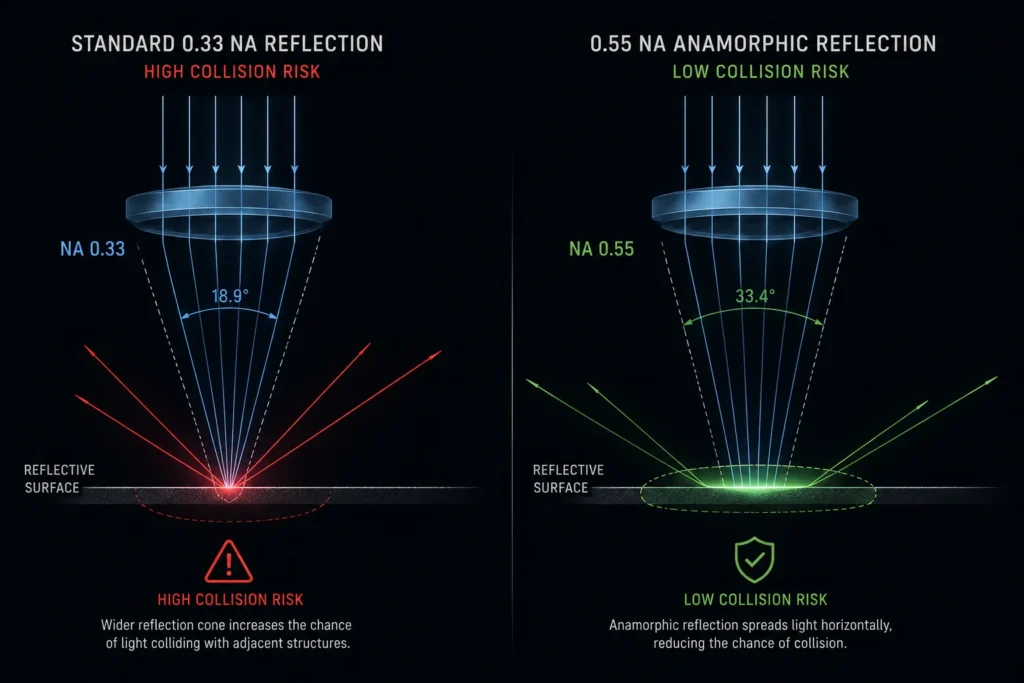
Here is where physics breaks down. EUV machines work by bouncing light off a reflective mask (the reticle) that holds the circuit pattern. If you make the mirrors bigger to catch the wider angles of light, the light coming in hits the light bouncing out. The angles overlap, creating a shadow.
4. Technical Depth: Anamorphic Optics
To stop the incoming and outgoing light from colliding, ASML had to increase the magnification of the mirrors so the light enters and exits at a steeper angle.
However, if you increase the magnification in all directions from 4x to 8x, the final chip you print shrinks by a factor of four. The “canvas” you can paint on becomes too small to fit modern, massive AI chips (like NVIDIA’s H100 or B200).
The brilliant, agonizing solution is Anamorphic Optics. The mirrors in a High-NA machine are shaped like funhouse mirrors. They magnify the light by 4x in the X-direction and 8x in the Y-direction. This prevents the light from colliding, but it introduces a massive new problem: the printed field size is cut strictly in half (from 26 x 33 mm to 26 x 16.5 mm).
5. Real-World Consequences: The Stitching Nightmare
Because the machine can only print half a chip at a time, to make a massive AI processor, the machine has to print the top half, physically move the silicon wafer, and perfectly “stitch” the bottom half to it. If the two halves are misaligned by the width of a few atoms, the $40,000 AI chip is ruined. Furthermore, because it prints smaller areas, the robotic stages holding the wafers have to accelerate at 8G (eight times the force of gravity) to maintain the factory’s output speed of 200 wafers per hour.
High-NA EUV Adoption: Intel vs. TSMC
The deployment of High-NA EUV is not a gradual rollout; it is a violent, high-stakes sprint among the top three semiconductor foundries on Earth.
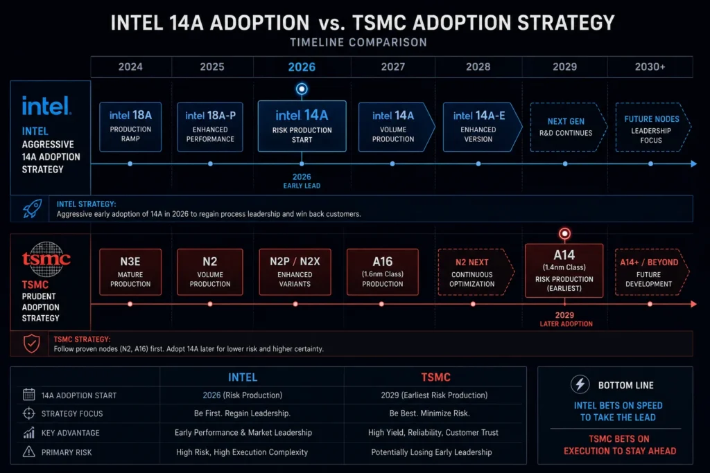
Intel (The First Mover): After losing its manufacturing crown to TSMC in the late 2010s, Intel CEO Pat Gelsinger made a massive bet. Intel was the very first company to purchase and install the ASML TWINSCAN EXE:5000. They are utilizing High-NA EUV as the bedrock of their upcoming Intel 14A manufacturing node (scheduled for late 2026/2027). By mastering the machine first, Intel aims to leapfrog TSMC and reclaim absolute leadership in transistor density.
TSMC (The Calculated Delay): Taiwan Semiconductor Manufacturing Company (TSMC), the current undisputed king of chipmaking, has taken a deeply contrasting approach. TSMC announced they will not use High-NA EUV for their upcoming A16 (1.6nm) node. Instead, they will squeeze every drop of capability out of their existing 0.33 NA machines using multi-patterning. They argue that the $350 million price tag of High-NA is currently too high to justify the economics, delaying their adoption until the end of the decade.
Advanced Memory (DRAM): While logic processors (CPUs/GPUs) get the headlines, memory is equally critical. Companies like Samsung and SK Hynix will eventually require High-NA EUV to print the increasingly microscopic capacitors required for next-generation High-Bandwidth Memory (HBM)—the memory chips that are physically stacked alongside NVIDIA GPUs to feed them data at terabytes per second.
Economic & Strategic Impact
The transition to High-NA EUV completely shatters the legacy cost curve of semiconductor foundries.
A leading-edge “Mega-Fab” currently costs roughly $20 billion to build. Integrating High-NA EUV pushes this closer to $30 billion. Because the machine prints half the field size (due to anamorphic optics), foundries may need to buy more machines to maintain the same volume of chip output.
This immense Capital Expenditure (CapEx) creates an inescapable consolidation effect. Twenty years ago, dozens of companies manufactured leading-edge chips. Today, there are exactly three: TSMC, Intel, and Samsung. No other company on Earth can afford a $350 million printer. The economics of High-NA EUV guarantee that the foundational hardware of the global AI economy will remain an impenetrable oligopoly for the foreseeable future.
Advantages
- Single-Patterning Precision: Allows foundries to print sub-2nm features in a single pass, drastically reducing manufacturing time and eliminating the microscopic alignment errors caused by double-patterning.
- Lower Defect Rates: Fewer passes through the lithography machine mean fewer opportunities for stray dust particles or chemical errors to ruin the silicon wafer.
- Enables Sub-2nm AI: Provides the physical resolution required to pack hundreds of billions of transistors onto a single piece of silicon, ensuring the continued scaling of advanced AI compute models.
Limitations
- The Half-Field Penalty: The anamorphic optics cut the printable chip size in half (26 mm x 16.5 mm). Modern AI chips (which are massive) must be “stitched” together, requiring flawless, atom-level robotic precision to align the two halves.
- Astronomical Costs: At roughly $350 million to $400 million per unit, the depreciation cost of the machine adds significant financial overhead to every single microchip produced.
- The Photoresist Bottleneck: Light is essentially a chemical trigger. The 0.55 NA lens focuses the light so tightly that the chemical layer on the wafer (the photoresist) struggles to react cleanly. The industry is currently scrambling to invent new metal-oxide photoresists that don’t blur under the intense, pinpoint energy of High-NA light.
Common Misconceptions
Misconception: High-NA uses a different, better type of laser.
Reality: The light source is identical to standard EUV (a high-power laser blasting droplets of molten tin 50,000 times a second to create 13.5nm plasma). The “High-NA” upgrade entirely concerns the mirrors that catch and focus the light, not the light itself.
Misconception: High-NA machines make the physical chips larger.
Reality: They do the exact opposite. Because of the funhouse-mirror anamorphic optics, the maximum size of a chip you can print in one shot is cut strictly in half.
Misconception: Moore’s Law is dead without High-NA.
Reality: Moore’s Law (the doubling of transistors) is surviving through 3D packaging (stacking chips on top of each other like a skyscraper). High-NA EUV simply keeps the 2D foundation of those skyscrapers shrinking. Both are required for the future of AI.
What Most People Miss
The violent physics of the Wafer Stage Acceleration.
Because the High-NA machine only prints half the area of an older machine, the factory’s output of chips per hour would theoretically be cut in half. To prevent this economic disaster, ASML had to redesign the robotic stage that holds the silicon wafer.
What most people miss is that the silicon wafer inside a High-NA machine is being violently thrown back and forth. The reticle stage accelerates at 32G, and the wafer stage accelerates at 8G. To put that in perspective, fighter pilots pass out at 9G. The machine is throwing a delicate piece of glass back and forth at eight times the force of gravity, stopping it with microscopic, nanometer-level precision, painting it with light, and throwing it again, hundreds of times a minute, without introducing a single vibration into the $350 million chassis.
Comparison Table
| Feature | Deep Ultraviolet (DUV) | Standard EUV (0.33 NA) | High-NA EUV (0.55 NA) |
| Wavelength (λ) | 193 nm | 13.5 nm | 13.5 nm |
| Numerical Aperture (NA) | Up to 1.35 (using water immersion) | 0.33 | 0.55 |
| Optics Type | Glass Lenses | Isomorphic Mirrors (4x) | Anamorphic Mirrors (4x/8x) |
| Exposure Field Size | 26 mm x 33 mm | 26 mm x 33 mm | 26 mm x 16.5 mm (Half size) |
| Machine Cost (Approx.) | $20M – $80M | $150M – $200M | $350M – $400M |
| Target Node | > 7nm | 7nm to 3nm | < 2nm (Intel 14A, TSMC A14) |
Case Study
Situation: Intel lost its undisputed leadership in semiconductor manufacturing around 2018 because it delayed the adoption of standard 0.33 NA EUV, believing it could push older DUV multi-patterning technology further. TSMC adopted EUV aggressively, resulting in vastly superior chips that allowed Apple and AMD to dominate the market.
Challenge: Intel CEO Pat Gelsinger initiated the “5 Nodes in 4 Years” turnaround strategy. To guarantee that Intel would not repeat the mistakes of the past, they needed to secure an insurmountable technological advantage for the sub-2nm era.
Solution (The High-NA Gamble): Intel committed to being the absolute first mover in High-NA EUV. They secured the very first TWINSCAN EXE:5000 machine from ASML, installing it in their Hillsboro, Oregon facility. They are currently calibrating their upcoming Intel 14A node specifically around the capabilities of the 0.55 NA optics.
Outcome: The strategy is a high-wire act. By adopting High-NA early, Intel incurs massive R&D costs to solve the “half-field” stitching and photoresist problems before anyone else. However, if they succeed, they will be able to print next-generation AI chips faster, cheaper, and with fewer defects than TSMC, who is delaying High-NA adoption to save on CapEx.
Lessons Learned: The case study proves that in leading-edge semiconductors, the risk of adopting new technology is astronomical, but the risk of delaying it is fatal. Intel’s entire corporate survival hinges on the bet that the physics of 0.55 NA anamorphic optics will yield a decisive commercial advantage before TSMC can successfully deploy the technology at scale.
Future Outlook
Next 12–24 Months
The era of Photoresist and Stitching Calibration. As Intel spins up the first High-NA machines for the Intel 14A node, the entire industry will be watching the defect rates. Over the next two years, chemical companies (like Tokyo Electron and JSR) will battle to perfect “Metal-Oxide Resists” (MOR)—specialized chemicals that can react to the incredibly sharp, pinpoint light of a 0.55 NA beam without blurring. Simultaneously, we will see the first commercial AI chips “stitched” together across the two half-fields, proving whether the robotic precision holds up in mass manufacturing.
Next 3–5 Years
The TSMC A14 Adoption Wave. While TSMC is skipping High-NA for their 1.6nm (A16) node, physics dictates they cannot hold out forever. By the end of the decade, as the industry pushes toward the A14 (1.4nm) and A10 (1nm) nodes, the cost of quadruple-patterning with standard EUV will finally exceed the $350 million cost of a High-NA machine. TSMC and Samsung will execute massive fleet upgrades, sparking an unprecedented revenue supercycle for ASML and cementing 0.55 NA as the undisputed global standard.
Next 10 Years
The theoretical limit: Hyper-NA (0.75 NA). What happens when 0.55 NA runs out of steam in the mid-2030s? ASML is already theoretically modeling “Hyper-NA” machines with a Numerical Aperture of 0.75. However, the optics required for 0.75 NA are so violently massive that the mirrors may not physically fit inside a standard fabrication facility. Pushing beyond 0.55 NA will likely require completely redesigning the architecture of a semiconductor plant from the ground up, pushing the cost of a single lithography machine well past the half-billion-dollar mark.
Most Likely Scenario
High-NA EUV is the final boss of 2D scaling. While the transition will be financially brutal and plagued with early yield issues, it is physically mandatory. The insatiable compute demands of Artificial General Intelligence (AGI) require transistors smaller than 2 nanometers. The 0.55 NA mirror is the only tool in the history of human engineering capable of drawing them.
Key Takeaways
- High-NA EUV lithography increases the Numerical Aperture (the size of the light-catching mirrors) from 0.33 to 0.55, allowing chips to be printed at sub-2nm resolutions.
- Because EUV light is absorbed by everything (including air and glass), the system uses a vacuum chamber and ultra-smooth mirrors to bounce and focus the light.
- To prevent the incoming light from crashing into the outgoing light on the larger mirrors, ASML used “anamorphic optics,” which stretches the light differently in the X and Y directions.
- This anamorphic trick solves the physics problem but cuts the printable chip size exactly in half, forcing machines to stitch two halves together to make massive AI chips.
- ASML is a global monopoly. They are the only company capable of building the machine, which costs roughly $350 million and weighs 150 tons.
- Intel is betting its corporate turnaround on being the first to master High-NA EUV, while TSMC is delaying adoption to save costs, creating a massive strategic divergence in the industry.
Glossary
Anamorphic Optics: A lens or mirror system that magnifies an image differently along its X and Y axes (like a funhouse mirror), used in High-NA EUV to prevent light beams from colliding.
Critical Dimension (CD): The smallest physical feature or line width that a lithography machine can reliably print on a silicon wafer.
EUV (Extreme Ultraviolet): Light with a wavelength of 13.5 nanometers. Because it is absorbed by almost all matter, it requires a vacuum environment and reflective mirrors rather than refractive glass lenses.
Numerical Aperture (NA): A dimensionless number that characterizes the range of angles over which a system can accept or emit light. A higher NA means a larger “lens” that captures more light, resulting in a sharper image.
Photoresist: A light-sensitive chemical coating applied to a silicon wafer. When EUV light hits it, the chemical changes, allowing the pattern of the microchip to be etched into the silicon below.
Rayleigh Criterion: A mathematical formula (CD = k₁ · (λ / NA) that defines the minimum resolvable detail a lithography system can achieve.
Frequently Asked Questions
Why can’t we just use a laser with a smaller wavelength instead of building bigger mirrors?
Creating the 13.5nm EUV light is already an act of extreme violence (blasting microscopic drops of tin with a massive laser). To go to a smaller wavelength (like X-rays), the light would pass straight through the mirrors instead of bouncing off them. We are currently stuck at 13.5nm, so we have to make the mirrors bigger.
If the machine only prints half a chip, how do they make big AI chips like the NVIDIA H100?
“Stitching.” The machine prints the top half of the blueprint, the robotic stage instantly shifts the wafer a few millimeters, and the machine prints the bottom half perfectly aligned with the top half. It requires atomic-level precision to ensure the microscopic wires line up across the seam.
How smooth are the mirrors inside the machine?
They are the smoothest objects ever created by human beings. Manufactured by Carl Zeiss, if you blew the mirror up to the size of the Earth, the tallest “mountain” on the mirror would be less than a millimeter high.
Who makes the High-NA machines?
ASML, a company headquartered in Veldhoven, Netherlands. They hold an absolute, 100% global monopoly on EUV technology. No other company or nation on Earth currently possesses the supply chain or patents to build one.
Is China building their own High-NA machines?
Currently, no. The US and Dutch governments heavily sanction ASML, preventing them from selling any EUV technology to China. While China is aggressively funding domestic lithography R&D, they are widely considered to be at least a decade away from replicating standard EUV, let alone High-NA EUV.
Sources
[1] ASML: High-NA EUV Lithography: Pushing the limits of Moore’s Law (2025/2026 Technology Briefs)
[2] IEEE Spectrum: The Anamorphic Optics Behind ASML’s High-NA EUV Lithography
[3] Intel Corporation: Intel 14A Node and the Transition to High-NA EUV Manufacturing
[4] Semiconductor Engineering: The Economic Realities of 0.55 NA EUV versus Multi-Patterning
[5] IMEC: EUV Lithography and the Challenge of Metal-Oxide Photoresists at High-NA