Advertisement
)
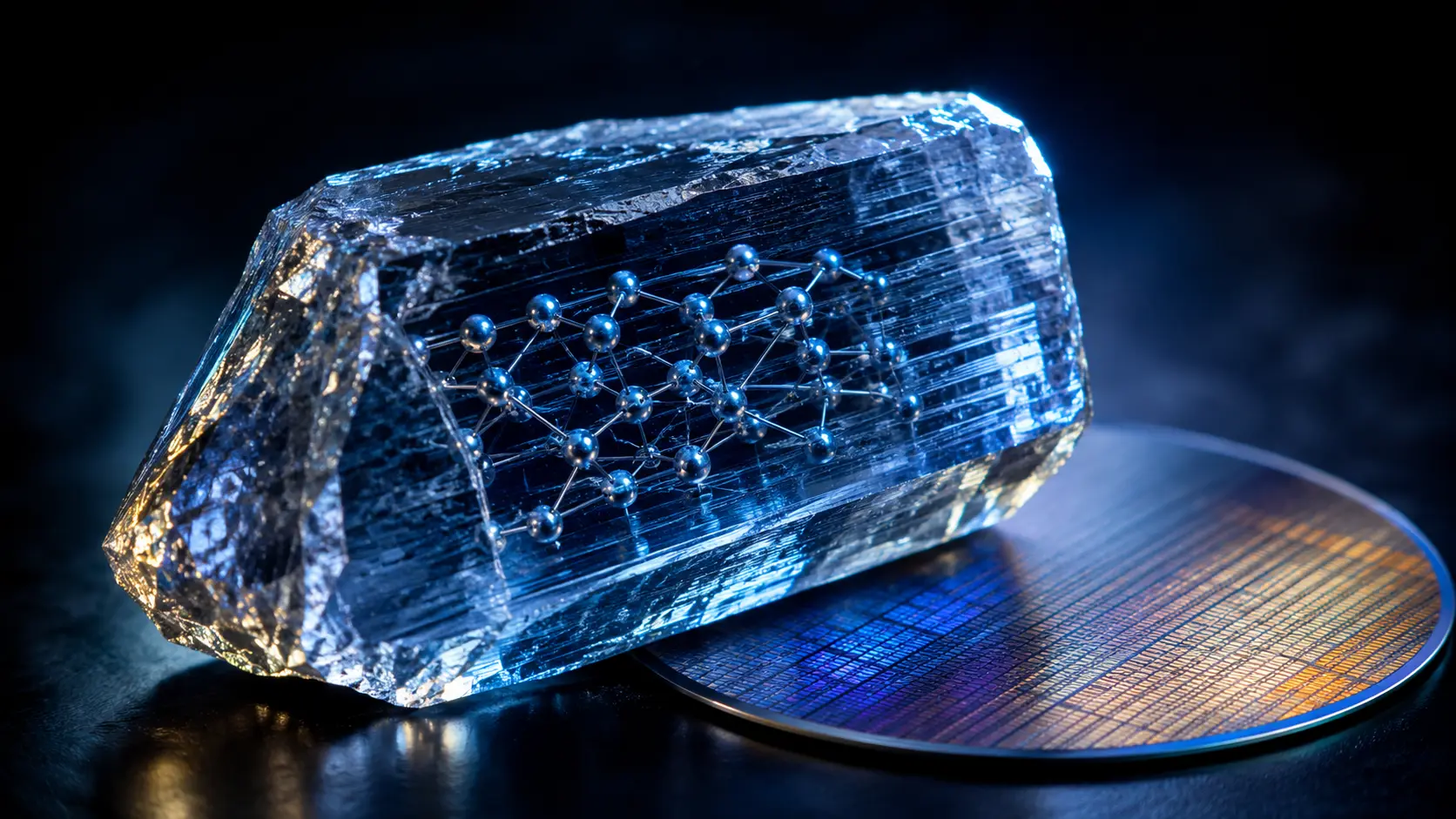

The electric vehicle revolution was built on the back of Silicon Carbide (SiC). By allowing power electronics to operate at higher voltages and temperatures, SiC unlocked faster charging and longer ranges. However, SiC is notoriously difficult to manufacture; growing a single crystal boule requires extreme vapor sublimation at 2,500°C, meaning the wafers are incredibly expensive and prone to defects. The global energy transition is desperate for a material that offers the extreme high-voltage performance of SiC, but can be manufactured with the cheap, rapid scalability of traditional silicon.
That material has arrived. Beta-phase Gallium Oxide (β-Ga2O3) has emerged as the definitive champion of the ultra-wide bandgap era. By mathematically crushing the performance limits of both SiC and Gallium Nitride (GaN), this obscure crystal allows engineers to build power switches that handle thousands of volts with virtually zero resistance. Why should you care right now? Because in early 2026, Japanese manufacturers successfully delivered the first 6-inch Gallium Oxide wafers, signaling the shift from laboratory R&D to commercial mass production. For hardware investors and supply chain analysts, this marks the beginning of the post-SiC generation, promising to drastically slash the cost of high-power electronics across global infrastructure.
What is Gallium Oxide Power Electronics?
Gallium Oxide power electronics utilize an ultra-wide bandgap semiconductor material, specifically beta-phase gallium oxide (β-Ga2O3), to manage extreme electrical voltages. Featuring a bandgap of 4.8 to 4.9 eV, it vastly outperforms silicon and silicon carbide in power switching applications and can be mass-produced cheaply using traditional melt-growth methods.
At a Glance
- Concept: Utilizing a synthetic crystal (β-Ga2O3) to build power transistors and diodes that can block immense voltages while conducting electricity with near-zero energy loss.
- Why it matters: It possesses a Baliga’s Figure of Merit (BFOM) of approximately 3,300, making it 3 to 10 times more theoretically capable than SiC and GaN.
- Who uses it: Electric vehicle manufacturers, utility-scale grid storage providers, and the U.S. Department of Defense for advanced radar and directed energy systems.
- Biggest takeaway: Unlike SiC, Gallium Oxide can be grown from a liquid melt using the exact same inexpensive techniques used to grow standard silicon, unlocking massive economies of scale.
In Simple Words
Think of a semiconductor as a dam holding back water (electricity).
Standard silicon is a wooden dam. It is incredibly cheap to build, but if the water pressure gets too high, the dam breaks. Silicon Carbide (SiC) is a reinforced concrete dam. It can hold back massive amounts of water, making it perfect for high-voltage electric vehicles, but pouring the concrete is a painfully slow and expensive process.
Gallium Oxide is a dam made of advanced titanium. It can hold back infinitely more pressure than the concrete dam, meaning you can build the dam walls much thinner and lighter. More importantly, engineers have figured out how to 3D-print this titanium dam just as quickly and cheaply as the original wooden one. It delivers the extreme high-performance required for the future of the power grid, without the paralyzing manufacturing costs of current-generation materials.
Why This Matters
The electrification of global transportation and heavy industry requires pushing power conversion systems past 1,200V and eventually 3,000V. Operating at these voltages pushes SiC to its absolute material limits, requiring thick, highly resistive drift layers that waste energy as heat.
For Semiconductor Engineers and Hardware VCs, Gallium Oxide is the definitive hardware arbitrage of the late 2020s. Ga2O3 devices rated above 3,000V could replace series-stacked configurations with single-device solutions. This architectural simplification reduces power conversion system complexity and slashes energy losses by 30% to 40%. Companies that secure the early supply chain for high-purity Ga2O3 substrates will effectively control the margin structure of the next decade’s power electronics market.
Global Market Growth for Gallium Oxide Semiconductors
The global gallium oxide market is experiencing an aggressive capital influx. Valued at $720.0 million in 2025, the market is projected to reach $789.84 million in 2026, and is forecast to expand to $1,993.45 million by 2036 at a 9.7% CAGR.
This growth reflects the critical transition of Ga2O3 from laboratory-scale crystal growth to early commercial substrate and device production. The market is bifurcated, with “Powders & Substrates” estimated to hold a 54.0% share in 2026, while end-use “Power Electronics” applications capture the remaining 46.0%. The United States currently leads global market growth with an 11.2% CAGR, heavily driven by defense infrastructure and semiconductor innovation grants.
How Gallium Oxide Power Electronics Work
Extracting extreme high-voltage performance while driving down substrate costs requires exploiting the unique crystallographic properties of the beta-phase. Here is the first-principles breakdown of the technology.
1. The Fundamental Problem: SiC Vapor Sublimation
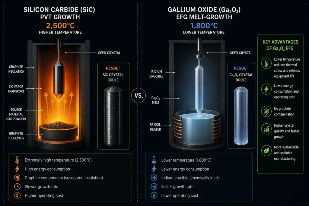
Manufacturing SiC wafers requires Physical Vapor Transport (PVT) at temperatures exceeding 2,500°C. The process is painfully slow, yielding small boules that suffer from high defect densities. This effectively puts a hard floor on how cheap SiC components can ever become.
2. The Core Mechanism: Melt-Growth Viability
Gallium oxide has five polymorphs, of which the beta phase (monoclinic) is thermodynamically stable and commercially relevant. Unlike SiC and GaN, Ga2O3 single crystals can be grown directly from a liquid melt using Czochralski, edge-defined film-fed growth (EFG), and floating zone methods at roughly 1,800°C. This enables manufacturers to pull large-diameter boules rapidly, at a fraction of the energy cost.
3. Technical Depth: The Ultra-Wide Bandgap
(Editor’s Note: To ensure WordPress compatibility and prevent the broken formula rendering issues observed in legacy uploads like image_7a0963.png, mathematical representations in this section are formatted using standard inline text rather than complex display blocks.)
Beta-Ga2O3 boasts a bandgap of 4.8 to 4.9 eV, significantly wider than SiC (3.3 eV) and GaN (3.4 eV). This extreme bandgap grants it a theoretical breakdown electric field of 8 MV/cm—nearly four times that of SiC and roughly ten times that of standard silicon. Because the material can block so much voltage, device engineers can design chips with dramatically thinner drift layers, heavily reducing conduction losses at blocking voltages above 1 kV.
4. Baliga’s Figure of Merit (BFOM)
To quantify this advantage, engineers rely on Baliga’s Figure of Merit (BFOM). The BFOM for β-Ga2O3 is approximately 3,300, which sits between 3 to 10 times higher than its SiC and GaN rivals. The BFOM directly governs how much voltage a device can block and how little energy it dissipates during conduction, making it the central benchmark for power device comparison.
5. Real-World Consequences: The Thermal Barrier
The primary physical penalty of Ga2O3 is its thermal dynamics. The market’s expansion is currently tempered by technical challenges, most notably the material’s inherently low thermal conductivity, which is only about one-tenth that of SiC. This creates severe heat dissipation hurdles for high-power applications, forcing engineers to develop advanced, top-side liquid cooling architectures to prevent the chips from melting themselves under load.
Commercial Applications of β-Ga2O3 Power Electronics
The transition from pure research to commercial deployment is targeting sectors where SiC is reaching its physical ceiling.
High-Voltage EV Powertrains: The electrification of transportation demands highly efficient on-board chargers and DC-DC converters. Ga2O3 enables smaller, vastly more efficient power conversion systems for 800V and 1,200V automotive architectures, directly extending the driving range of electric vehicles.
Directed Energy and Radar Electronics: The aerospace and defense sectors are aggressive early adopters, utilizing 99.9999% (6N) purity Ga2O3 for satellite power, radar electronics, and military avionics. The U.S. Department of Defense’s DARPA WIDE program funded over twenty university and industry research programs focused on Ga2O3 device fabrication since 2022, with cumulative grant disbursements estimated at $340 million through 2025.
Deep-Ultraviolet (DUV) Photodetectors: Beyond power applications, high purity Ga2O3 is finding growing adoption in deep-ultraviolet (DUV) photodetectors. Because of its 4.8 eV bandgap, it is completely transparent to visible light but highly responsive to DUV spectrums, making it ideal for flame detection, missile plume warning systems, and gas-sensing arrays for industrial safety.
Economic & Strategic Impact
The strategic commercialization timeline relies entirely on scaling wafer diameters to lower the unit economics per die.
In late 2024, Novel Crystal Technology officially launched commercial 1200 V Ga2O3 Schottky barrier diodes, confirming the material’s transition to near-commercial product status. The critical breakthrough occurred in early 2026, when Novel Crystal Technology announced the delivery of 150mm (6-inch) β-Ga2O3 wafer samples.
This 6-inch milestone proves that the melt-growth advantage is real and scalable. Novel Crystal Technology has established a definitive roadmap: delivering 150mm epitaxial wafers by 2027, achieving full-scale mass production by 2029, and pushing toward 200mm (8-inch) wafers in 2035. This aggressive scale-up threatens to heavily undercut the pricing power of legacy SiC foundries by the end of the decade.
Advantages
- Extreme Voltage Tolerance: Features a theoretical breakdown electric field of 8 MV/cm, allowing for massive voltage blocking in an ultra-thin chip footprint.
- Melt-Growth Manufacturing: Single crystals can be grown from liquid melt (Czochralski and EFG methods), enabling significantly cheaper, large-diameter wafer production compared to SiC vapor sublimation.
- Unmatched BFOM: Possesses a Baliga’s figure of merit of roughly 3,300, vastly outperforming both SiC and GaN in theoretical power efficiency.
Limitations
- Severe Thermal Bottleneck: The material’s thermal conductivity is exceptionally poor (roughly one-tenth that of SiC), requiring heavy investments in advanced heat-sinking and active cooling to prevent chip failure.
- P-Type Doping Challenges: Unlike silicon, β-Ga2O3 is extremely difficult to p-dope, largely restricting current commercial architectures to unipolar devices like Schottky barrier diodes and specific FET topologies.
- Immature Supply Chain: Despite rapid growth, the global supply of 6-inch wafers is still in the sampling phase as of 2026, meaning hyperscale fab deployment remains several years away from matching the mature capacity of the current SiC ecosystem.

Comparison Table
| Feature | Silicon Carbide (SiC) | Beta-Gallium Oxide (β-Ga2O3) |
| Bandgap | 3.3 eV | 4.8 – 4.9 eV |
| Breakdown Field | ~2.5 MV/cm | 8.0 MV/cm |
| Baliga’s Figure of Merit | Baseline Benchmark | ~3,300 (3-10x higher) |
| Crystal Growth Method | Vapor Sublimation (Expensive) | Melt-Growth (Scalable/Cheap) |
| Thermal Conductivity | Extremely High | Very Low (~1/10th of SiC) |
| Current Wafer Size (2026) | 8-inch (200mm) widespread | 6-inch (150mm) samples delivered |
Case Study
Situation: The global push for energy efficiency demanded power electronic components capable of handling voltages exceeding 1,200V without massive energy loss. Silicon Carbide (SiC) emerged as the stopgap, but its prohibitive manufacturing costs and physical limits created a ceiling for ultra-high-voltage grid applications.
Challenge: Producing an ultra-wide bandgap material that outperformed SiC thermodynamically, while completely bypassing the slow, expensive vapor sublimation crystal growth process.
Solution (The 6-Inch Milestone): Japanese manufacturer Novel Crystal Technology (NCT) targeted the unique melt-growth capabilities of beta-phase gallium oxide. In early 2026, NCT successfully initiated the delivery of 150mm (6-inch) β-Ga2O3 wafers specifically designed for next-generation power semiconductors.
Outcome: This breakthrough in wafer size officially transitioned Ga2O3 from a laboratory novelty to a viable mass-production asset. NCT cemented a commercial roadmap to deliver epitaxial wafers in 2027 and reach full-scale mass production by 2029 using low-cost growth methods.
Lessons Learned: The achievement proved that superior power density does not mandate superior manufacturing costs. By leveraging legacy silicon-style melt-growth techniques, the semiconductor industry successfully established a cheaper, more powerful successor to SiC, redefining the baseline metrics for the power electronics market.
Future Outlook
Next 12–24 Months
The era of Epitaxial Refinement and Commercial Sampling. Throughout 2026 and 2027, the focus will remain squarely on improving the epitaxial quality of 6-inch wafers. Tier-1 automotive OEMs and grid-storage providers will begin rigorous qualification testing of 600V to 1,200V MOSFETs and Schottky barrier diodes provided by startups in the U.S. and Japan.
Next 3–5 Years
The Mass Production and Cooling Integration Phase. By 2029, Novel Crystal Technology and its global competitors will hit full-scale mass production of β-Ga2O3. During this window, the thermal conductivity bottleneck will be addressed through advanced packaging. The industry will widely adopt aggressive wafer-thinning techniques and direct double-sided liquid cooling to manage the intense heat generated by Ga2O3 chips, allowing them to be safely installed in consumer EV powertrains.
Next 10 Years
The transition to 3,000V+ Grid Domination. By the mid-2030s, the global market will mature, reaching a projected value near $2 billion. As manufacturers achieve the 200mm (8-inch) wafer milestone around 2035, the economy of scale will allow Ga2O3 to completely displace SiC in high-voltage industrial automation and national renewable energy grids. Devices rated above 3,000V will dramatically simplify power conversion systems, cementing Gallium Oxide as the definitive foundation of the zero-carbon grid.
Most Likely Scenario
Gallium Oxide is executing the exact disruption playbook that SiC used against standard silicon a decade ago. While its extreme thermal limitations require novel engineering workarounds, the sheer mathematical superiority of its 4.8 eV bandgap and its massive melt-growth cost advantage make it an unstoppable force in the ultra-high-voltage semiconductor market.
Key Takeaways
- Beta-phase Gallium Oxide (β-Ga2O3) is an ultra-wide bandgap semiconductor material boasting a bandgap of 4.8 to 4.9 eV, enabling extreme high-voltage power devices.
- It offers a theoretical breakdown electric field of 8 MV/cm, nearly four times that of Silicon Carbide (SiC).
- Its Baliga’s Figure of Merit (BFOM) is roughly 3,300, drastically outperforming SiC and GaN by 3 to 10 times in theoretical efficiency.
- Crucially, Ga2O3 can be grown cheaply from a liquid melt using Czochralski and EFG methods, avoiding the expensive vapor sublimation required for SiC.
- In early 2026, Novel Crystal Technology delivered 6-inch wafer samples, targeting full-scale mass production by 2029.
- The primary commercial barrier is the material’s extremely low thermal conductivity (roughly one-tenth of SiC), requiring highly advanced packaging for heat dissipation.
Glossary
Baliga’s Figure of Merit (BFOM): A critical mathematical benchmark that defines how much voltage a semiconductor device can block versus how little energy it dissipates during conduction.
Bandgap: The energy range in a solid where no electron states can exist. An “ultra-wide” bandgap allows a material to withstand massive voltages without breaking down and short-circuiting.
Beta Phase (β-Ga2O3): The monoclinic polymorph of gallium oxide. It is the most thermodynamically stable form of the crystal and the primary focus for commercial power electronics.
Breakdown Electric Field: The maximum electric field strength a material can endure before it fails and begins conducting electricity uncontrollably.
Czochralski / EFG Methods: Legacy “melt-growth” techniques used to rapidly pull large, single-crystal boules from a pool of liquid material, allowing for cheap, large-scale wafer manufacturing.
Schottky Barrier Diode (SBD): A semiconductor diode formed by the junction of a semiconductor with a metal, widely used in power electronics for fast switching with low forward voltage drops.
Sources
- Fact.MR: Gallium Oxide Market | Global Market Analysis Report – 2036
- Dataintelo: High Purity Gallium Oxide (Ga2O3) Market Research Report 2034
- Patsnap: Gallium oxide power semiconductor landscape 2026
- Patsnap: Gallium oxide: 4.9 eV bandgap vs SiC and GaN
- 36氪 (36Kr): Gallium Oxide: On the Brink of a Groundbreaking Breakthrough
- 24MarketReports: Gallium Oxide Single Crystal Substrate Market 2026 forecast to 2032