Advertisement
)


The global energy transition has a severe geopolitical and thermodynamic choke point: the silicon wafer. To build a standard solar panel, raw quartz must be smelted in 1,500°C furnaces to forge ultra-pure polysilicon ingots—a massive, capital-intensive industrial process heavily concentrated in a single geopolitical bloc. Furthermore, the physics of silicon have hit a hard mathematical ceiling. The best commercial silicon panels are maxing out at roughly 26% efficiency. This means nearly three-quarters of the sun’s energy hitting a panel is wasted as useless heat or passes straight through.
Why should you care right now? Because materials scientists have engineered a way to abandon the heavy silicon wafer entirely. By utilizing synthetic crystals known as perovskites, engineers can tune the exact “color” of light the material absorbs. Instead of one thick slab of silicon, they are stacking two microscopic, specialized perovskite layers on top of each other. This “All-Perovskite Tandem” architecture doesn’t just shatter the efficiency ceiling of traditional solar panels—it fundamentally rewrites the economics of manufacturing. Because these crystals can be dissolved into liquid inks, gigawatts of highly efficient, flexible solar panels can now be printed continuously on giant roll-to-roll printing presses, entirely bypassing the multi-billion-dollar silicon supply chain.
What are All-Perovskite Tandem Solar Cells?
All-Perovskite Tandem Solar Cells are photovoltaic devices that stack a wide-bandgap perovskite top layer and a narrow-bandgap perovskite bottom layer. This eliminates the need for a silicon base. The architecture absorbs a broader spectrum of sunlight, achieving efficiencies over 30%, and can be manufactured via low-cost, roll-to-roll liquid printing.
At a Glance
- Concept: Stacking two different solar cells on top of each other. The top cell catches the high-energy blue light, and the bottom cell catches the low-energy red light.
- Why it matters: Silicon panels waste massive amounts of energy because high-energy photons create heat instead of electricity. The tandem architecture stops this thermal waste, breaking the theoretical limits of standard solar power.
- Who uses it: Cutting-edge research institutions (Nanjing University, UNSW), commercialization startups (Renshine Solar, Oxford PV), and major energy conglomerates evaluating flexible photovoltaics.
- Biggest takeaway: Because both layers are made of perovskite (rather than one perovskite layer and one rigid silicon layer), the entire dual-layer solar panel can be printed as a thin, flexible film, turning solar manufacturing from heavy metallurgy into high-speed printing.
In Simple Words
Imagine you are trying to catch fish in a fast-moving river.
A Standard Silicon Solar Cell is like using a single, medium-sized net. It catches medium fish perfectly. But the tiny fish slip right through the holes, and the massive, high-speed fish hit the net so hard they break it, causing the net to heat up and waste energy. Because of this, you only ever catch about 26% of the fish in the river.
An All-Perovskite Tandem Cell uses two nets stacked behind each other.
The first net (the Top Cell) is incredibly strong and has large holes. It catches the massive, high-speed fish effortlessly without breaking or heating up, letting the smaller fish pass safely through.
Right behind it is a second net (the Bottom Cell) with incredibly fine mesh. It catches all the tiny fish that passed through the first net.
By stacking the nets, you catch both the massive fish and the tiny fish, increasing your total haul past 30%. Because these “nets” are made of perovskite ink, you don’t need a heavy steel frame to hold them; you can just paint them onto a flexible sheet of plastic.
Why This Matters
For Clean-Tech Investors and Energy Planners, all-perovskite tandems represent the ultimate Capital Expenditure (CapEx) disruption.
Building a modern 10-Gigawatt silicon solar cell factory requires billions of dollars of heavy metallurgical equipment: quartz smelters, Czochralski crystal pullers, diamond wire saws, and high-vacuum deposition chambers. It is a slow, batch-based manufacturing process.
All-perovskite tandems are manufactured using “solution processing.” The raw materials are dissolved into solvents and coated onto a continuous, moving roll of flexible substrate (Roll-to-Roll or R2R manufacturing) [1]. This transition from batch-smelting to continuous-printing slashes the factory footprint and the initial CapEx by an estimated 80%. It enables western nations to rapidly spin up domestic, gigawatt-scale solar manufacturing without attempting to compete with Asia’s entrenched polysilicon monopoly.
The Evolution of Perovskite-Silicon Tandems
The solar industry has spent the last five years heavily focused on Perovskite-Silicon Tandems. Companies like LONGi set massive world records (35.5% in 2026) by painting a single layer of perovskite on top of a standard silicon cell [4].
While Perovskite-Silicon is an excellent bridge technology, it remains anchored to the heavy, rigid, energy-intensive silicon wafer. The true endgame of the photovoltaic roadmap is the All-Perovskite Tandem. By removing silicon entirely, the industry unlocks Building-Integrated Photovoltaics (BIPV)—solar cells so light and flexible they can be laminated onto curved skyscrapers, electric vehicle roofs, and deployed on lightweight drones, vastly expanding the total addressable market for solar energy generation.
How All-Perovskite Tandem Solar Cells Work
Bypassing the Shockley-Queisser limit using two liquid-printed crystals requires extreme bandgap engineering. Here is the first-principles breakdown of the architecture.
1. The Fundamental Problem: Thermalization Losses
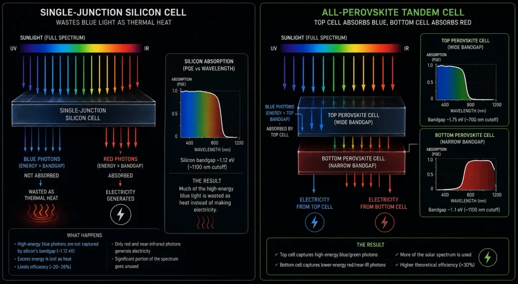
In a single-junction silicon cell (Bandgap ≈ 1.1 eV), photons with exactly 1.1 eV of energy are converted efficiently into electricity [2]. However, if a high-energy blue photon (e.g., 2.5 eV) hits the cell, the extra 1.4 eV is instantly wasted as heat (“thermalization”) [2]. This heat buildup limits the absolute maximum theoretical efficiency of silicon to 33.7% [3, 5].
2. The Core Mechanism: Bandgap Tuning
Perovskites are unique because their bandgap can be chemically “tuned.” By altering the ratio of halides (Iodine vs. Bromine) and metals (Lead vs. Tin) in the liquid precursor ink, engineers can dictate exactly what color of light the crystal absorbs [1, 2].
An all-perovskite tandem stacks two different crystals:
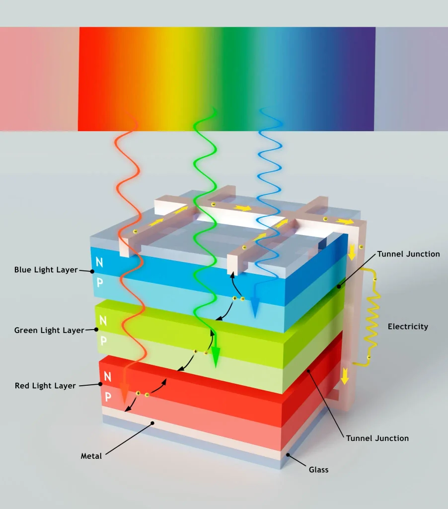
- The Top Cell (Wide-Bandgap): Tuned to ≈ 1.8 eV. It absorbs the high-energy blue and green light at very high voltages, preventing the energy from being wasted as heat. It is transparent to red and infrared light.
- The Bottom Cell (Narrow-Bandgap): Tuned to ≈ 1.2 eV. It catches the low-energy red and infrared light that passed straight through the top cell.
3. Technical Depth: Light-Induced Halide Segregation (The Hoke Effect)
To get the top cell to a wide 1.8 eV bandgap, engineers must mix Bromine and Iodine in the crystal lattice. However, when sunlight hits this mixed-halide crystal, a catastrophic failure known as the “Hoke effect” occurs. The light causes the Bromine and Iodine to physically separate (segregate) [1, 2].
This segregation creates microscopic “pools” of low-bandgap iodine. The electrical charge gets trapped in these pools, causing the voltage of the solar panel to plummet under intense sunlight.
4. Mitigating the Hoke Effect
To stop halide segregation, materials scientists deploy A-Site Cation Alloying. By mixing heavy elements like Cesium (Cs) or Formamidinium (FA) into the crystal structure, the lattice stiffens. This internal thermodynamic strain-relief locks the Bromine and Iodine into place, ensuring the wide-bandgap perovskite remains completely stable under sustained, blazing sunlight [1, 2].
5. Real-World Consequences: The Recombination Layer
Between the top and bottom perovskite cells lies the “Interconnect Layer” or “Tunnel Junction.” The electrons generated by the top cell must flawlessly recombine with the “holes” generated by the bottom cell. If this ultra-thin layer is poorly printed, electrical resistance spikes, destroying the efficiency of the tandem. Engineers use atomic-level coatings of transparent conductive oxides (like Indium Tin Oxide) mixed with organic passivators to ensure the two printed crystals pass electricity between each other with zero friction [3].
Commercial Deployments: BIPV and Flexible Solar
While still transitioning out of the laboratory, the unique properties of all-perovskite tandems target markets where heavy silicon fundamentally fails.
Aerospace and High-Altitude Pseudo-Satellites (HAPS): Stratospheric drones and low-earth-orbit satellites require solar panels with an extreme “Power-to-Weight Ratio” (Watts per kilogram). Silicon panels are heavy and require rigid glass protection. Because all-perovskite tandems are printed on ultra-thin flexible polymers, they generate massive amounts of power while weighing practically nothing, keeping surveillance and communication drones aloft indefinitely.
Building-Integrated Photovoltaics (BIPV): Modern architecture demands seamless energy integration. Because the perovskite ink can be semi-transparent or tinted by tweaking the bandgap, manufacturers can print these tandem cells directly into the glass of skyscraper windows or as flexible decals that wrap around the curved surfaces of commercial buildings, generating gigawatts of urban power without ugly roof racks.
Agrivoltaics (Dual-Use Farming): Traditional silicon panels cast dark, opaque shadows, rendering the land underneath them useless for crop growth. Tunable perovskite panels can be engineered to absorb only the specific light frequencies not utilized by the underlying plants for photosynthesis. This allows farmers to suspend flexible, semi-transparent solar canopies over their fields, generating high-yield electricity while simultaneously sheltering crops from extreme heat and preserving soil moisture.
Economic & Strategic Impact
The core strategic value of all-perovskite tandems is the Democratization of Cell Manufacturing.
The current silicon supply chain is a rigid, centralized monopoly. A nation cannot easily spin up a silicon wafer industry because the barriers to entry (cheap electricity for smelting, established metallurgical ecosystems, massive environmental permitting) take decades to build.
All-perovskite roll-to-roll manufacturing operates fundamentally like a newspaper printing press or a packaging film plant. The capital expenditure is drastically lower, and the chemical precursors (iodine, lead, formamidinium) are globally ubiquitous and inexpensive. This allows Europe, the United States, and emerging economies to build massive, localized solar manufacturing hubs in months rather than years, securing domestic energy independence and insulating their grids from global trade wars and tariff embargoes.
Advantages
- Extreme Efficiency Potential: The theoretical limit of a two-junction all-perovskite tandem approaches 47%, and certified lab prototypes have already crossed the 30% barrier, drastically outperforming standard silicon [2, 5].
- Low-Temperature Processing: Silicon requires 1,500°C furnaces. Perovskite inks are processed and crystallized at temperatures well below 150°C, drastically reducing the energy required to manufacture the solar panel itself.
- Mechanical Flexibility: By eliminating the brittle silicon wafer, the entire tandem stack can be printed on flexible substrates (like PET plastic), allowing the panels to be rolled, bent, and easily transported.
- Bandgap Tunability: The exact light-absorption properties of the top and bottom cells can be chemically dialed in to perfectly match the local solar spectrum or specific architectural requirements.
Limitations
- Operational Stability: Perovskite crystals are highly sensitive to moisture, oxygen, and intense heat. While “T80” degradation metrics have vastly improved in the lab (passing 1,000 hours), proving that a flexible, plastic-encapsulated module can survive 25 years of real-world rain and hail remains the primary hurdle for commercialization [1, 3].
- Lead Toxicity: The highest-performing perovskites contain water-soluble lead. If a solar panel is shattered in a hail storm, there is a regulatory concern that lead could leach into the soil. While the total volume of lead is microscopic, it presents a stringent environmental and public relations barrier.
- Tin Oxidation in the Bottom Cell: The narrow-bandgap bottom cell requires Tin (Sn) instead of Lead. Tin naturally wants to oxidize (rust) from Sn²⁺ to Sn⁴⁺ when exposed to even trace amounts of air during manufacturing. This oxidation instantly ruins the cell’s efficiency, demanding excruciatingly strict, oxygen-free manufacturing environments.
Common Misconceptions
Misconception: “Tandem solar cell” always means replacing silicon.
Reality: The vast majority of commercial tandem news today focuses on Perovskite-Silicon tandems (putting one layer of perovskite on top of a standard silicon panel). The All-Perovskite tandem is a different, more advanced architecture that removes silicon entirely.
Misconception: The efficiency records are for massive, roof-sized panels.
Reality: The 30%+ world records are currently achieved on “hero cells”—microscopic squares often smaller than a postage stamp (1 cm²) [3]. Translating that perfect 30% efficiency to a massive, meter-wide roll-to-roll sheet without introducing microscopic coating defects is the central engineering challenge.
Misconception: Perovskites are rare-earth minerals that must be mined.
Reality: Perovskite is a crystal structure, not a specific mined mineral. The materials used to make solar perovskites are inexpensive, abundant, synthetically produced laboratory chemicals.
What Most People Miss
The disruptive intelligence value of Defect Passivation at the Tunnel Junction.
When analyzing tandem cells, observers focus heavily on the bandgaps of the top and bottom crystals. What most miss is the invisible atomic battleground between the two layers.
If you just stack two perovskites, the interface between them becomes riddled with “defects” (missing atoms or microscopic cracks). These defects trap the electricity before it can leave the panel. The true breakthrough driving recent 30% world records isn’t just the crystals; it is the invention of advanced organic passivators (like piperazinium iodide or PDAI) [3]. These chemicals are painted at the junction, acting as a molecular glue that perfectly heals the defects at the grain boundaries, allowing the electrical current to bridge the gap between the two layers with zero friction.
Comparison Table
| Feature | Single-Junction Silicon | Perovskite-Silicon Tandem | All-Perovskite Tandem |
| Material Base | Rigid Polysilicon Wafer | Silicon base + Perovskite top | Two Perovskite ink layers |
| Theoretical Efficiency Limit | 33.7% [3, 5] | ~43% [4] | ~47% [5] |
| Current World Record | 26.8% [2] | 35.5% (LONGi, 2026) [4] | 30.1% (Nanjing/Renshine) [2] |
| Manufacturing Temp | > 1,500°C | High | < 150°C |
| Form Factor | Rigid, Heavy | Rigid, Heavy | Ultra-lightweight, Flexible |
| Commercial Status | 95% of Global Market [2] | Early Commercial Rollout [1, 5] | Advanced R&D / Pilot Lines |
Case Study
Situation: As the solar industry hit the thermodynamic limits of single-junction silicon, the race to break the 30% efficiency barrier became paramount. While perovskite-silicon hybrids crossed this line, they remained burdened by the heavy, inflexible, and expensive silicon wafer supply chain.
Challenge: Develop a highly efficient, dual-layer solar architecture completely devoid of silicon. This required perfectly tuning a wide-bandgap top cell that wouldn’t degrade under sunlight (the Hoke effect) and a narrow-bandgap bottom cell that wouldn’t instantly oxidize during the manufacturing process.
Solution (The 30% Barrier Breakthrough): In early 2024, a collaborative effort by Nanjing University and Renshine Solar tackled the all-perovskite tandem architecture. They heavily engineered the A-site cations in the wide-bandgap top cell to suppress light-induced halide segregation. Crucially, they developed a novel, defect-healing recombination layer (tunnel junction) to seamlessly fuse the top cell to the tin-lead mixed narrow-bandgap bottom cell without creating electrical resistance.
Outcome: The architecture resulted in an all-perovskite tandem solar cell achieving an independently certified efficiency of 30.1% on a standardized test area [2]. This milestone was globally significant; it proved definitively that two layers of printed, solution-processed crystals could mathematically and practically outperform the finest, heavily smelted silicon wafers ever manufactured.
Lessons Learned: The achievement validated that the future of photovoltaics relies on multi-junction structures, but confirmed that silicon is no longer a mandatory foundation. By mastering the chemical interfaces between the stacked layers, the researchers proved that gigawatt-scale, ultra-efficient solar energy can theoretically be printed on flexible plastic at room temperature.
Future Outlook
Next 12–24 Months
The era of Roll-to-Roll Process Optimization. The immediate horizon will focus intensely on translating the 30% “postage-stamp” lab records into uniform, large-area module production. R&D capital will pour into slot-die coating and gravure printing technologies designed to lay down massive sheets of perovskite ink without a single microscopic pinhole. Startups will heavily target niche, high-margin markets (like aerospace, drone power, and indoor IoT charging) where the ultra-lightweight, flexible nature of the all-perovskite cell commands a massive price premium over heavy silicon.
Next 3–5 Years
The scaling of Encapsulation and Durability Certification. As manufacturing yields improve, the existential battle will be surviving the IEC 61215 certification—the brutal industry standard for 25-year solar panel weather resistance. Materials scientists will introduce advanced Atomic Layer Deposition (ALD) barriers and highly robust polymer laminates to permanently seal the flexible tandems against water vapor and oxygen. We will see the first major commercial deployments of all-perovskite BIPV (Building-Integrated Photovoltaics), transforming urban skyscraper facades into silent, invisible power plants.
Next 10 Years
The Utility-Scale Decoupling. By the mid-2030s, the operational lifespan of all-perovskite tandems will be definitively validated in the field. This will trigger a massive structural shift in global energy procurement. Because printing rolls of perovskite is exponentially cheaper than smelting silicon, the Levelized Cost of Energy (LCOE) for solar will plummet yet again. Utility-scale solar farms will begin deploying massive, ultra-cheap “roll-out” solar carpets, completely upending the geopolitical dominance of the established Asian polysilicon supply chain and decentralizing global solar manufacturing.
Most Likely Scenario
All-Perovskite Tandems represent the final, thermodynamically optimal architecture for terrestrial solar energy. While rigid perovskite-silicon hybrids will dominate the immediate transition phase, the sheer economic gravity of zero-silicon, low-temperature, roll-to-roll manufacturing guarantees that all-perovskite thin films will eventually overtake the market. They are not just better solar panels; they are a fundamental rewiring of how the planet harvests its primary energy source.
Key Takeaways
- Standard silicon solar panels waste nearly 70% of sunlight as heat and are maxed out around 26% efficiency.
- “Tandem” solar cells stack two different layers on top of each other. The top layer catches high-energy blue light, and the bottom layer catches low-energy red light, boosting efficiency past 30%.
- While most companies are currently sticking a perovskite layer on top of a rigid silicon panel, the ultimate goal is the “All-Perovskite Tandem”—using two layers of perovskite and completely deleting the silicon.
- Because perovskites are liquid inks, all-perovskite tandems can be printed on flexible plastic using high-speed roll-to-roll printing presses, drastically crashing the cost of manufacturing.
- The technology overcomes major hurdles, including the “Hoke effect,” where sunlight causes the chemicals in the wide-bandgap top cell to separate and lose power.
- By eliminating the need for 1,500°C silicon smelting factories, all-perovskite tandems allow nations to build cheap, localized solar manufacturing hubs, bypassing centralized global supply chains.
Glossary
A-Site Cation Alloying: Mixing different molecular elements (like Cesium) into the perovskite crystal to make it physically tougher and prevent it from degrading under intense sunlight.
Bandgap: The specific amount of energy a material requires to absorb a photon and turn it into electricity. A material’s bandgap dictates what “color” of light it catches.
Building-Integrated Photovoltaics (BIPV): Solar panels that are built directly into the architecture of a building (like tinted, energy-generating windows) rather than bolted onto the roof.
Hoke Effect (Light-Induced Halide Segregation): A failure in mixed-perovskites where intense sunlight causes the internal chemicals (bromine and iodine) to separate, ruining the solar cell’s voltage.
Roll-to-Roll (R2R) Manufacturing: A high-speed, continuous manufacturing process where liquid materials (like perovskite ink) are painted onto a moving, flexible sheet of plastic or foil.
Shockley-Queisser Limit: The absolute mathematical limit of efficiency for a standard, single-layer solar cell (roughly 33.7%).
Thermalization Loss: The energy wasted when a high-energy photon hits a low-bandgap solar cell. The excess energy is turned into useless heat rather than electricity.
Sources
[1] PMC. (2020). Strain-activated light-induced halide segregation in mixed-halide perovskite solids.
[2] Fluxim. (2026). Highest Perovskite Solar Cell Efficiencies (2026 Update).
[3] PatSnap. (2026). Perovskite-silicon tandem solar cells hit 34% in 2026.
[4] LONGi Green Energy Technology. (2026). 35.5%! LONGi Once Again Breaks World Record for Crystalline Silicon-Perovskite Tandem Solar Cell Efficiency.
[5] PatSnap. (2026). Perovskite-silicon tandem solar cells hit 34% in 2026 (Industry Analysis).