Advertisement
)
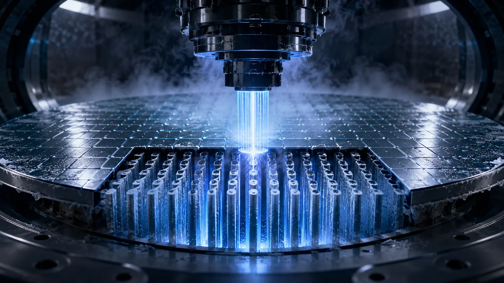

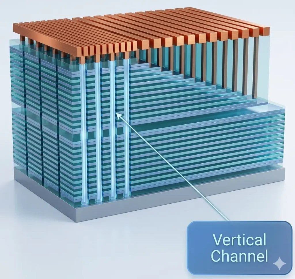
To fit a terabyte of data into a smartphone, semiconductor manufacturers can no longer build microchips horizontally. They build them vertically, stacking microscopic memory cells into staggering silicon skyscrapers. Today, a leading-edge 3D NAND flash memory chip is effectively a 300-story building. To wire these floors together, engineers must drill “memory holes”—microscopic vertical trenches that plunge straight down through every single layer.
Why should you care right now? Because we have hit the physical limit of how deep we can drill. As manufacturers push toward 400 and 500 layers, the trenches have become so incredibly deep and narrow that traditional plasma etching fails. The plasma scatters, carving out the sides of the trench and causing the silicon skyscraper to cave in on itself. To bypass this geometric crisis, the semiconductor industry is abandoning room-temperature manufacturing. By freezing the silicon wafer to cryogenic temperatures—plunging it below -60°C—engineers alter the fundamental thermodynamics of the plasma gas. This extreme deep-freeze allows for perfectly straight, 10-micron-deep holes to be drilled at record speeds, permanently unblocking the roadmap for next-generation data storage.
What is Cryogenic Dielectric Etching?
Cryogenic Dielectric Etching is an advanced semiconductor manufacturing process used to carve extreme high-aspect-ratio (HAR) trenches in 3D NAND memory chips. By cooling the silicon wafer to sub-zero temperatures (e.g., -60°C), the process alters the chemical adsorption of plasma gases, preventing lateral erosion and ensuring perfectly vertical, microscopic holes.
At a Glance
- Concept: Freezing a silicon microchip to sub-zero temperatures so that the chemical gases used to drill microscopic holes behave differently, creating perfectly straight, ultra-deep trenches.
- Why it matters: Traditional drilling methods fail when the holes get too deep; they bulge in the middle or clog at the top. Cryogenic etching prevents this, allowing memory chips to be stacked 400+ layers high.
- Who uses it: Global memory giants (Samsung, SK Hynix, Micron) and leading semiconductor equipment manufacturers (Tokyo Electron, Lam Research, Applied Materials).
- Biggest takeaway: Etching these deep holes normally takes hours and creates a massive traffic jam in the factory. Cryogenic etching does it in exactly 33 minutes, doubling the output of a multi-billion-dollar semiconductor fab.
In Simple Words
Imagine you are trying to use a blowtorch to dig a perfectly straight, incredibly deep well through a massive block of wax.
If you do this at Room Temperature, the heat from the blowtorch doesn’t just melt the bottom of the well; it melts the sides, too. The walls of your well bulge out, the hole gets warped, and eventually, the wax collapses in on itself before you reach the bottom.
If you use Cryogenic Etching, you plunge the entire block of wax into a deep freeze. Now, when you fire the blowtorch straight down, the intense, focused heat still melts the bottom. But because the surrounding wax is freezing cold, any heat that strays sideways is instantly neutralized. The walls stay perfectly frozen and rock-solid. You can dig an infinitely deep, perfectly straight well in a fraction of the time without worrying about a cave-in.
Why This Matters
For Semiconductor Engineers, Hardware VCs, and Supply Chain Analysts, the transition to cryogenic etching resolves the ultimate Capital Expenditure (CapEx) Bottleneck.
Building a modern memory fab costs upwards of $15 billion. The most expensive tools on the factory floor are the High-Aspect-Ratio (HAR) dielectric etchers. Because drilling a 300-layer memory hole at room temperature is agonizingly slow (often taking several hours per wafer), these etching machines create a massive logistical traffic jam. Fabs are forced to buy rows upon rows of these $10M+ machines just to keep production moving.
Cryogenic etching completely disrupts this math. By fundamentally changing the chemistry of the plasma, the etch rate increases by over 200%. A wafer that previously sat in a chamber for two hours is now finished in 33 minutes. This allows a semiconductor manufacturer to drastically increase their wafer output without expanding the physical size of their cleanroom, fundamentally lowering the cost-per-bit of global data storage.
The Evolution of 3D NAND: Beating the Aspect Ratio
The evolution of 3D NAND is defined by the struggle against the Aspect Ratio.
Aspect ratio is the relationship between the depth of a hole and its width. A standard coffee cup has an aspect ratio of roughly 1:1. The memory holes in early 3D NAND chips had an aspect ratio of 40:1. Today, as layer counts exceed 300, these microscopic holes have aspect ratios of over 100:1 and are approaching 150:1. Navigating highly reactive plasma ions down a microscopic 150:1 canyon without them hitting the walls and destroying the chip is considered one of the hardest feats in modern mechanical and chemical engineering.
How Cryogenic Dielectric Etching Works
Achieving a perfectly vertical profile at a 150:1 aspect ratio requires abandoning traditional polymer chemistry in favor of thermodynamics. Here is the first-principles breakdown of the architecture.
1. The Fundamental Problem: Lateral Etching and Bowing
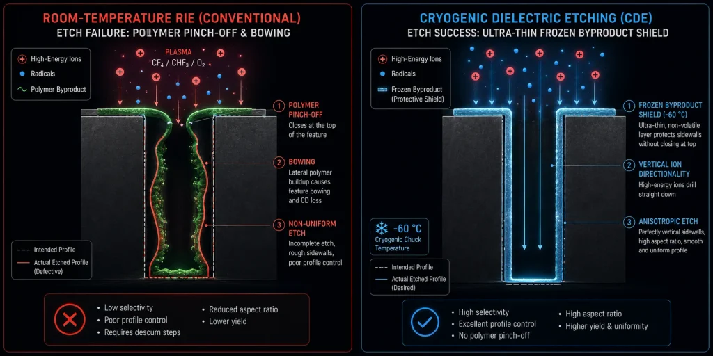
In a traditional Reactive Ion Etch (RIE), a plasma gas is accelerated downward by an electric field to bombard and carve the silicon. However, some ions naturally scatter sideways. If they hit the sidewall, they etch it laterally. In a 300-layer chip, this lateral etching creates a fatal defect called “bowing”—the middle of the trench bulges outward, potentially merging with the adjacent memory hole and short-circuiting the chip.
2. The Insufficiency of Room-Temperature Passivation
To prevent bowing at room temperature, engineers use heavy fluorocarbon gases (like C₄F₆ or C₄F₈). These gases form a thick, Teflon-like polymer coating on the sidewalls as the hole is drilled, acting as a shield. But in extreme high-aspect-ratio (HAR) trenches, the polymer-forming gas struggles to reach the bottom. It builds up too heavily at the top of the hole, causing it to “pinch-off” and clog before the etch is finished.
3. The Core Mechanism: The Cryogenic Chuck
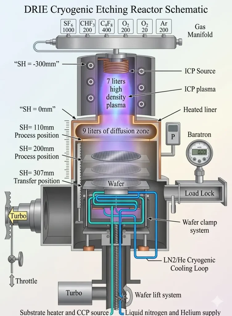
To bypass the polymer problem, the equipment manufacturer upgrades the electrostatic chuck (the platter that holds the wafer). Using advanced liquid coolants, the chuck plunges the silicon wafer’s temperature down to -60°C or colder.
4. Technical Depth: Physisorption vs Chemisorption
By freezing the wafer, the physics of the sidewall protection change entirely. At cryogenic temperatures, the system no longer needs thick, heavy fluorocarbon polymers to protect the walls. Instead, it relies on Physisorption.
As the plasma etches the silicon at the bottom of the hole, it releases chemical byproducts (such as SiF₄). Because the walls of the trench are freezing cold, these specific byproducts literally condense and freeze onto the sidewalls, forming an ultra-thin, localized “ice” shield.
5. Real-World Consequences: Extreme Anisotropic Velocity
This temporary, frozen shield protects the sidewalls from scattered ions perfectly. Crucially, because the vertical ions bombarding the bottom of the hole carry high kinetic energy, they blast right through the thin ice layer at the floor of the trench, allowing the downward etch to continue unhindered.
Because the system no longer has to carefully balance the slow injection of thick polymers, engineers can aggressively crank up the ion energy. The etch plunges straight downward at blinding speeds, resulting in a perfectly straight (anisotropic) profile with zero bowing and zero pinch-off.
Commercializing Cryogenic Etch: Tokyo Electron (TEL)
The theoretical elegance of cryogenic plasma chemistry is now fully operational, fundamentally redefining the capabilities of tier-one memory foundries.
Single-Tier vs. Multi-Tier Architecture: When manufacturers first hit the memory hole bottleneck around 128 layers, they were forced to adopt “string stacking” or multi-tier architectures. They would etch a 64-layer hole, fill it, stack another 64 layers on top, and etch again, carefully aligning the two microscopic holes. This alignment is agonizingly difficult and ruins yields. Cryogenic etching allows fabs to delay string stacking. By enabling ultra-deep etching in a single pass, fabs can execute a 200+ layer chip in a “single-tier,” drastically simplifying the manufacturing flow and increasing profitability.
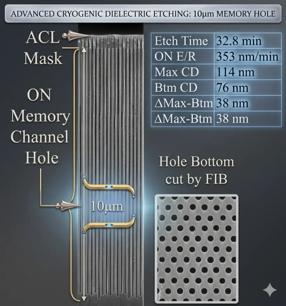
Tokyo Electron’s Breakthrough: In mid-2023, Tokyo Electron (TEL), one of the world’s premier semiconductor equipment manufacturers, announced a paradigm-shifting cryogenic etch technology. Utilizing their specialized plasma chambers and extreme cooling, they successfully demonstrated a 10 µm deep memory hole etch with a high-aspect-ratio profile in just 33 minutes. This specific technological leap was widely heralded as the definitive key required to unlock the 400-layer 3D NAND generation.
Reducing Global Warming Potential (GWP): The traditional room-temperature etch process relies heavily on perfluorocarbons (PFCs) like CF₄, C₄F₆, and C₄F₈. These gases have an exceptionally high Global Warming Potential (thousands of times worse than CO₂) and linger in the atmosphere for millennia. Because cryogenic etching fundamentally alters the passivation mechanism, it reduces the reliance on these aggressive, thick polymer-forming greenhouse gases. Foundries can utilize alternative, lower-GWP gas chemistries (such as specialized SF₆ and Hydrogen mixes) that perform efficiently only at sub-zero temperatures, drastically improving the ESG profile of the semiconductor facility.
Economic & Strategic Impact
The core strategic disruption is the Preservation of the Moore’s Law Cost Curve.
While Moore’s Law technically refers to transistor density, the economic corollary is that the cost per gigabyte of memory must continuously fall. If manufacturers were forced to rely on room-temperature etching for 400-layer chips, the etch times would mathematically require a doubling of fab floor space just to house the necessary machinery. The cost to build a gigabyte of flash memory would suddenly increase, breaking a 40-year economic trend.
Cryogenic etching prevents this inversion. By accelerating the etch rate by a factor of 2.5x to 3x, the capital efficiency of the existing fab footprint is preserved. It guarantees that the 2 Terabyte smartphones and ultra-dense enterprise SSDs of the late 2020s will reach the consumer market at highly accessible price points.
Advantages
- Massive Throughput Increases: Etch times are reduced from multiple hours to tens of minutes, radically improving wafer-per-hour (WPH) output for the most expensive tool in the fab.
- Perfect Anisotropic Profiles: Physisorption of byproducts at sub-zero temperatures prevents lateral sidewall attacks, completely eliminating bowing, twisting, and pinch-off defects.
- Enhanced Mask Selectivity: The “hard mask” (the template placed on top of the wafer) degrades rapidly at room temperature. At cryogenic temperatures, the mask erodes much slower, allowing for deeper etching without the mask wearing away entirely.
- Simplified Single-Tier Manufacturing: Delays the need for highly complex, low-yield “string stacking” by allowing hundreds of layers to be pierced in a single, continuous step.
Limitations
- Extreme Thermal Stress: Cycling a vacuum chamber and an electrostatic chuck down to -60°C or -100°C requires immensely complex liquid cooling loops and advanced metallurgy. The sheer thermal stress on the hardware leads to increased maintenance requirements and potential machine downtime.
- Condensation and Ice Defect Risks: Operating an ultra-cold surface inside a vacuum chamber creates a severe risk of unwanted condensation. If trace amounts of moisture or rogue gas particles freeze onto the wafer before the etch begins, it acts as a microscopic “boulder,” blocking the plasma and ruining the memory hole.
- Wafer Thermal Shock: Rapidly moving a fragile, 300mm silicon wafer from a warm factory environment onto a sub-zero chuck can induce thermal shock, potentially warping the wafer or causing the delicate, hundreds-of-layers-thick ONON stacks to delaminate.
Common Misconceptions
Misconception: The process uses lasers to drill the hole.
Reality: While lasers are used in lithography to draw the blueprint, the actual digging of the deep 3D NAND trench is done entirely by a chaotic storm of charged plasma ions bombarding the silicon.
Misconception: Freezing the silicon makes it brittle so it shatters more easily.
Reality: The freezing temperature has almost no mechanical effect on the structural integrity of the solid silicon lattice. The cold temperature is entirely about controlling the behavior of the gases and byproducts floating in the chamber.
Misconception: Once etched, the memory chip is finished.
Reality: Drilling the hole is only half the battle. Once the 400-layer trench is perfectly excavated, engineers must then use Atomic Layer Deposition (ALD) to paint the inside of that microscopic canyon with specialized conductive and insulating materials, exactly one atom layer at a time.
What Most People Miss
The disruptive intelligence value of Dynamic Profile Tuning (DPT).
Most analysts assume the wafer is simply held at a static -60°C for the entire 33-minute process. What they miss is the precise, real-time thermodynamic choreography required as the hole gets deeper.
When a trench is 1 micron deep, the gas behaves differently than when the trench is 9 microns deep. Advanced cryogenic etch platforms utilize Dynamic Profile Tuning. The machine actively and continuously adjusts the temperature of the electrostatic chuck by fractions of a degree, while simultaneously modulating the ion energy and gas flow ratios in real-time. This dynamic interplay ensures that the delicate “frozen” passivation layer maintains the exact optimal thickness required, continuously adapting to the changing physics of the hole as it plunges deeper toward the substrate.
Comparison Table
| Feature | Room-Temperature RIE | Cryogenic Dielectric Etching |
| Wafer Temperature | +20°C to +60°C | -60°C to -100°C |
| Sidewall Protection | Thick Fluorocarbon Polymer | Condensed Byproducts (Physisorption) |
| Etch Rate | Slow (Diffusion limited) | Extremely Fast (2x – 3x improvement) |
| Profile Defects | High risk of bowing and twisting | Perfectly anisotropic (straight) |
| Mask Selectivity | Moderate to Poor | Excellent |
| Environmental Impact | Relies on high-GWP fluorocarbons | Can utilize low-GWP gas chemistries |
Case Study
Situation: To meet the explosive demand for enterprise cloud storage, a leading tier-one memory manufacturer targeted a transition to a >300-layer 3D NAND architecture. However, early pilot lines relying on room-temperature etching faced catastrophic yield failures. The heavy fluorocarbon gases required to protect the upper sidewalls of the 120:1 aspect ratio trenches were completely choking off the tops of the holes, leaving the bottom 50 layers entirely unetched.
Challenge: Develop an etching regime capable of maintaining a perfectly straight, anisotropic profile down to 10 microns without clogging the aperture, while simultaneously reducing the total etch time to prevent a multi-billion-dollar bottleneck on the factory floor.
Solution (The Sub-Zero Transition): The foundry partnered with equipment providers to install specialized Deep Reactive Ion Etching (DRIE) chambers equipped with advanced cryogenic electrostatic chucks. They transitioned the recipe away from heavy, polymerizing fluorocarbons toward a leaner gas mixture, dropping the wafer temperature below -60°C.
Outcome: The thermodynamics of the cryogenic environment allowed the immediate byproducts of the silicon etch to physically freeze to the sidewalls, creating a micron-perfect, self-regulating protective shield. The ions successfully reached the absolute bottom of the >300-layer stack. The total processing time plummeted from nearly two hours to under 35 minutes, completely unblocking the pilot line and allowing the foundry to yield the world’s first single-tier, ultra-high-density storage chips.
Lessons Learned: The deployment validated that brute-force mechanical power (higher plasma energy) is useless without absolute thermodynamic control. By manipulating the phase state of the chemical byproducts via extreme cold, the industry proved that the geometric limits of silicon scaling can be overridden by mastering the micro-environments of the vacuum chamber.
Future Outlook
Next 12–24 Months
The era of Mainstream Cryo-Adoption. In the immediate term, cryogenic dielectric etching will transition from leading-edge pilot lines to high-volume manufacturing standard operating procedures. As memory giants officially commercialize their 300+ layer NAND architectures (like Samsung’s V9 or Micron’s 232+ layer nodes), the presence of sub-zero cooling loops will become ubiquitous across global fabrication plants, dictating the capital expenditure cycles of the equipment sector.
Next 3–5 Years
The scaling of Ultra-Cryo and Dual-Tier Alignment. As the industry relentlessly marches toward 400 and 500 layers, even cryogenic etching will hit a physical depth limit for a single pass. Foundries will be forced back to “dual-tier” architectures—drilling 250 layers, and stacking another 250 on top. The industry will push the cryogenic chucks even colder (approaching -100°C) to drill these individual tiers faster and cleaner, focusing heavily on minimizing the mechanical stress that could disrupt the microscopic alignment of the upper and lower tiers.
Next 10 Years
The Cryogenic Logic Crossover. By the mid-2030s, the profound profile control demonstrated in 3D NAND will bleed over into standard logic microprocessors (CPUs and GPUs). As logic chips adopt Backside Power Delivery Networks (BSPDN), engineers must drill incredibly deep, straight “Through-Silicon Vias” (TSVs) to route power from the bottom of the chip. The cryogenic etching techniques mastered in the memory sector will become the foundational methodology for wiring the multi-layered, 3D-stacked AI logic processors of the future.
Most Likely Scenario
Cryogenic Dielectric Etching is not merely an incremental upgrade; it is the definitive savior of the vertical scaling roadmap. By effectively pausing the chaotic chemical reactions on the sidewalls of a microscopic trench, sub-zero manufacturing has rescued the semiconductor industry from an insurmountable geometric wall. As the hunger for generative AI data storage accelerates, the ability to freeze silicon to near absolute zero will be the quiet, unheralded champion keeping the digital economy afloat.
Key Takeaways
- To increase storage capacity, memory chips are stacked over 300 layers high, requiring microscopic holes to be drilled straight down through the entire silicon structure.
- Traditional room-temperature plasma drilling takes hours and often fails because the protective gases clog the top of the hole or carve out the sides, causing the chip to cave in.
- Cryogenic Dielectric Etching solves this by freezing the silicon chip to sub-zero temperatures (below -60°C).
- Because the walls of the microscopic hole are freezing, the chemical dust created by the drilling instantly freezes to the walls, creating a perfect, microscopic “ice shield” that stops the hole from bowing outward.
- This thermodynamic trick allows engineers to use higher-energy plasma to drill straight down at blinding speeds, cutting the manufacturing time from over two hours to just 33 minutes.
- The technology is the absolute prerequisite for building 400-layer and 500-layer 3D NAND flash memory, permanently unblocking the global data storage roadmap.
Glossary
Anisotropic: A process that etches in only one direction (straight down), resulting in perfectly vertical walls without any sideways (lateral) erosion.
Aspect Ratio: The ratio of a trench’s depth to its width. Drilling a 100:1 aspect ratio hole is like digging a well 100 feet deep but only 1 foot wide.
Bowing: A fatal manufacturing defect where the plasma strays sideways, carving out the middle of the trench so it bulges outward, potentially ruining the microchip.
Chemisorption vs Physisorption: Chemisorption requires a complex chemical reaction to stick to a surface (used in room temp etching). Physisorption relies purely on physical condensation/freezing (used in cryogenic etching).
Reactive Ion Etching (RIE): The standard method of carving silicon. A machine creates a stormy cloud of charged plasma gas and fires the ions downward like microscopic bullets to blast away the material.
Throughput / Wafers Per Hour (WPH): The financial heartbeat of a semiconductor factory. Cryogenic etching triples the WPH of the most expensive machine in the building.
Sources
Tokyo Electron (TEL): Breakthrough in High Aspect Ratio Etch using Cryogenic Technology
Journal of Vacuum Science & Technology: Cryogenic etching of high aspect ratio silicon structures
Applied Materials: Overcoming the Challenges of 3D NAND Scaling
Semiconductor Engineering: The Shift to Cryogenic Etching in Advanced Memory
Lam Research: Advancements in Dielectric Etch for 3D NAND Architectures