Advertisement
)

The semiconductor industry has a physics problem, and it is trying to solve it with money. To make microchips faster, engineers must draw increasingly microscopic lines on silicon wafers. Currently, the only way to draw a 2-nanometer line is to use an Extreme Ultraviolet (EUV) lithography scanner—a $350 million, bus-sized machine that blasts molten tin with a laser to generate a wavelength of light that barely exists in nature. However, as these lines get thinner, the light begins to fail. Because light is made of individual particles (photons), shining an EUV laser at a 2nm scale is like spraying a wall with a shotgun. It creates jagged, rough edges and broken wires known as “stochastic defects.” The optical approach to Moore’s Law is hitting a fundamental thermodynamic wall.
Why should you care right now? Because materials scientists are abandoning optics for chemistry. Instead of using a $350 million laser to carve lines from the top down, the industry is reviving a breakthrough technology called Directed Self-Assembly (DSA). By pouring a specialized liquid polymer onto a silicon wafer and baking it, the chemicals are thermodynamically forced to organize themselves into perfect, perfectly straight nanoscale wires. This “bottom-up” manufacturing technique doesn’t just fix the jagged errors caused by EUV light; it mathematically multiplies the resolution of older, cheaper microchip factories. DSA threatens to radically slash the capital expenditure required to build the next generation of artificial intelligence hardware.
What is Directed Self-Assembly (DSA)?
Directed Self-Assembly (DSA) is a semiconductor nanofabrication technique that utilizes the thermodynamic properties of block copolymers. When applied to a silicon wafer and annealed, these polymers naturally phase-separate into highly ordered, nanoscale geometric patterns. Guided by pre-existing chemical or physical templates, DSA achieves ultra-high resolution patterning without requiring expensive advanced optical lithography.
At a Glance
- Concept: Using chemicals that naturally want to separate (like oil and water) to automatically draw perfectly straight, microscopic lines on a computer chip.
- Why it matters: The machines currently used to draw these lines cost $350 million each and are reaching their physical limits. DSA can achieve the same or better resolution for a fraction of the cost.
- Who uses it: Premier semiconductor research hubs (IMEC), materials suppliers (Merck, Brewer Science), and Tier-1 foundries (Intel, TSMC, Samsung).
- Biggest takeaway: DSA isn’t just about drawing new lines; it’s about fixing bad ones. Foundries are using DSA polymers to “iron out” the jagged, broken lines created by expensive EUV lasers, healing the chip at a molecular level.
In Simple Words
Imagine you need to paint perfectly straight, alternating black and white stripes on a highway, but your paintbrushes are too wide, and your hands are too shaky.
This is the problem with current microchip manufacturing. The light (the paintbrush) is getting too messy to draw microscopic wires perfectly.
Directed Self-Assembly (DSA) is like inventing a magical bucket of mixed black and white paint. You just dump the bucket onto the highway. Because the black paint and the white paint chemically repel each other—but are magnetically tied together—they cannot separate into random puddles. Instead, as the paint dries, it automatically forces itself into perfectly straight, razor-thin, alternating black and white stripes. You didn’t have to paint the stripes; the chemistry did the work for you. You just had to tell the paint where to start.
Why This Matters
For Semiconductor Engineers, Hardware VCs, and Materials Scientists, DSA is the ultimate CapEx Evasion and Pitch Multiplication strategy.
If a foundry wants to shrink a 40nm wire into four 10nm wires, they traditionally have to use “Multi-Patterning.” They must run the silicon wafer through a $150 million lithography machine four separate times, executing dozens of highly toxic etching and deposition steps. This takes days and ruins profitability.
With DSA “Pitch Multiplication,” the foundry runs the wafer through the cheap machine exactly once, drawing a single, cheap 40nm trench. They pour the DSA polymer into the trench. The polymer automatically separates into four perfect 10nm lines. The foundry achieved 10nm resolution using 40nm equipment, completely bypassing the need to purchase High-NA EUV scanners for that specific chip layer.
Bottom-Up Nanofabrication vs. Top-Down Lithography
The history of semiconductor manufacturing is entirely “Top-Down.” You take a block of silicon and carve away what you don’t want using light and acid. DSA introduces “Bottom-Up” manufacturing. You allow the molecules to grow and organize themselves into the structure you desire.
While bottom-up nanotechnology has been a sci-fi dream for decades, it was historically too chaotic to use in commercial computers. DSA bridges the gap. By using traditional “Top-Down” lithography to provide a macroscopic scaffold, and “Bottom-Up” polymers to fill in the microscopic details, the industry achieves the precision of chemistry with the reliability of heavy engineering.
How Directed Self-Assembly (DSA) Uses Block Copolymers
Forcing random liquid polymers to assemble into a flawless 10-nanometer logic gate requires manipulating the deep thermodynamics of macromolecular physics. Here is the first-principles breakdown of the architecture.
1. The Fundamental Problem: Photon Shot Noise
In Extreme Ultraviolet (EUV) lithography, the light wavelength is 13.5nm. Because the photons carry so much energy, there are very few of them. When these scarce photons hit the photoresist chemical on the wafer, they strike it randomly (stochastically), like raindrops on pavement. This randomness leaves the edges of the printed wire looking jagged and rough (Line-Edge Roughness, or LER). At 2nm, a jagged edge causes the wire to short-circuit.
2. The Core Mechanism: Block Copolymers (BCPs)
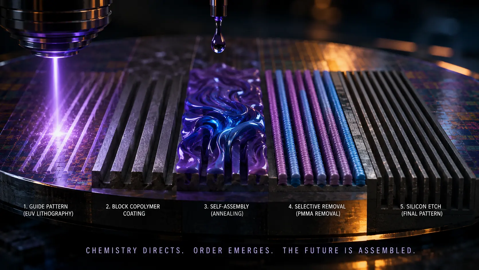
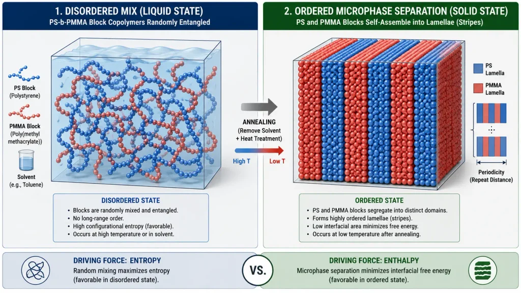
DSA abandons light and relies on Block Copolymers. The most common is PS-b-PMMA (Polystyrene tethered to Poly(methyl methacrylate)). These two polymer chains fundamentally repel each other—they want to separate. However, because they are covalently bonded together, they cannot separate completely.
3. Technical Depth: Microphase Separation and the χ Parameter
When the wafer is heated (annealed), the polymers enter a mobile state. To minimize their thermodynamic free energy, they arrange themselves into alternating nanostructures (like lamellae/stripes or cylinders). The size and sharpness of these stripes are dictated by the Flory-Huggins interaction parameter (χ, pronounced “chi”). A higher χ means the two polymers hate each other more, resulting in sharper, smaller, tighter patterns.
4. Directing the Assembly: Epitaxy
If you just pour the polymer on a flat wafer, it forms a useless, chaotic fingerprint pattern. To make useful computer chips, the assembly must be directed.
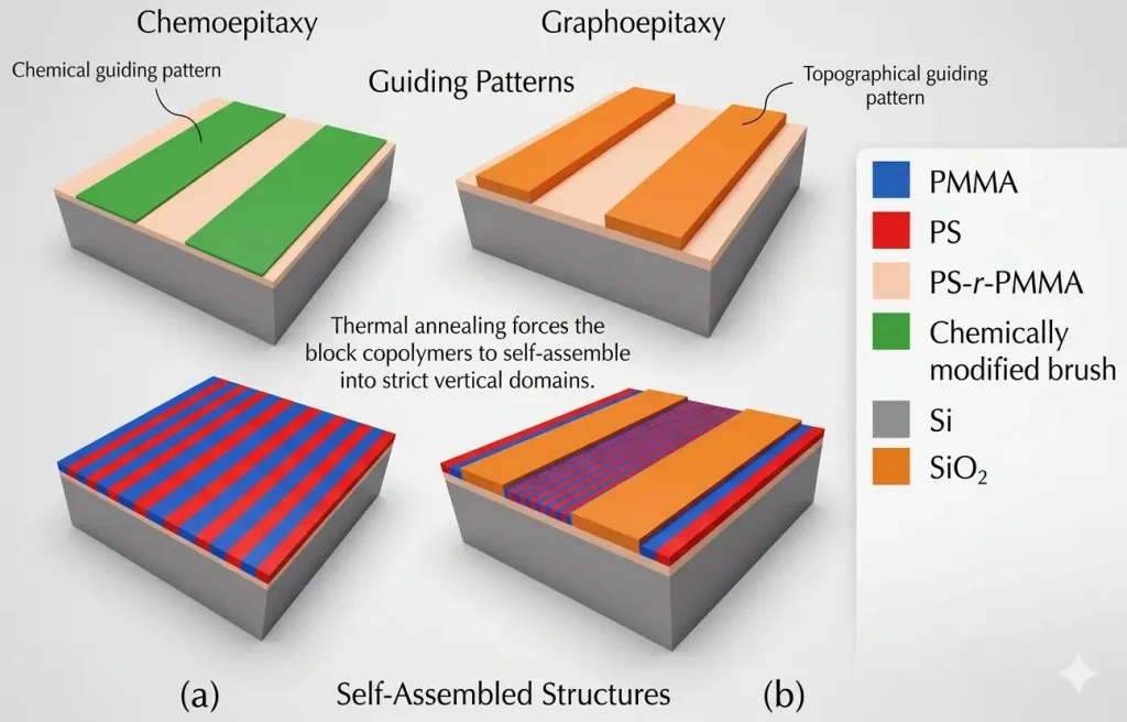
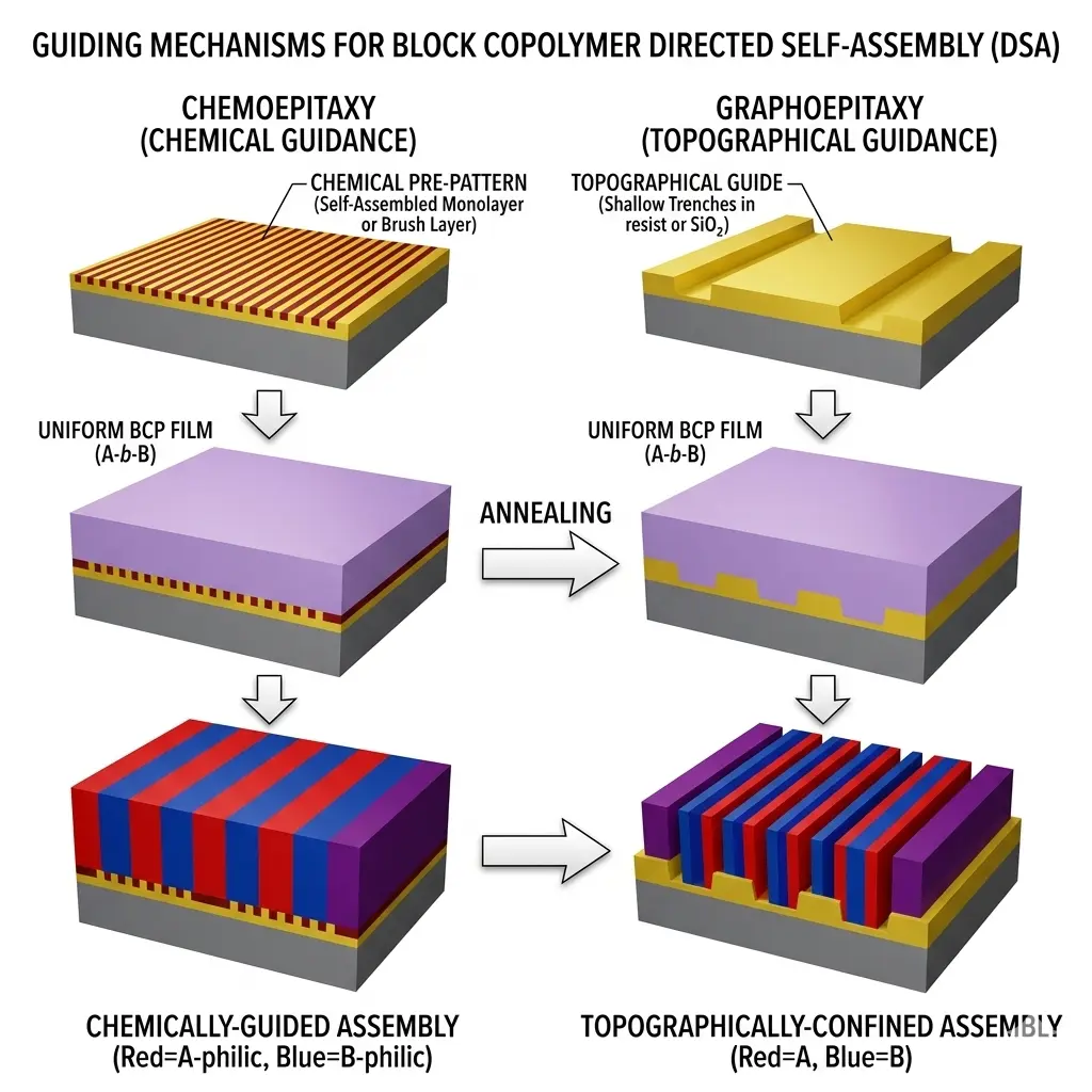
- Grapho-epitaxy: The foundry uses standard lithography to carve physical trenches (walls) into the silicon. The polymer is poured inside. The walls physically force the polymers to align parallel to the trench.
- Chemo-epitaxy: The foundry lays down flat, alternating stripes of chemicals (a “brush” layer). One chemical stripe attracts the PS polymer, the other attracts the PMMA. The polymer binds to this chemical blueprint and aligns perfectly.
5. Real-World Consequences: PMMA Removal
Once the wafer cools, you have perfectly alternating stripes of PS and PMMA. The final step is to hit the wafer with a specific plasma or UV light that instantly dissolves the PMMA, but leaves the PS intact. The PMMA washes away, leaving behind a flawless, nanoscale stencil of PS. The foundry then uses standard acid etching to carve this exact 10nm pattern deep into the underlying silicon.
Commercial DSA Use Cases: DRAM and EUV Rectification
While DSA was heavily hyped in the 2010s, it failed early commercialization because the defect rates were too high. Today, ultra-pure chemistry has resurrected the technology for specific, highly lucrative commercial chokepoints.
DRAM Contact Hole Shrinking: Memory chips (DRAM) require billions of perfectly uniform, microscopic circular holes (contact holes) packed tightly together. Standard lithography struggles to print perfect circles at nanoscale; they often look like blurry ovals. By printing a slightly larger, blurry oval, and dropping a cylinder-forming block copolymer inside, the polymer thermodynamically organizes into a perfect, mathematically exact sub-nanometer circle. This “Contact Hole Shrink” is the most mature, immediate commercial application of DSA in global memory foundries.
EUV Rectification (Defect Healing): The most profound application of DSA today is not replacing EUV, but fixing it. When a $350M EUV scanner prints a jagged, flawed 3nm line, the foundry can coat that flawed line with a thin layer of DSA polymer. The thermodynamics of the polymer force it to smooth itself out, physically “ironing” the jagged edges of the EUV line into a perfectly straight, robust wire before the final silicon etch. This rectification rescues massive silicon wafers that would otherwise be thrown in the trash.
Bit-Patterned Media (Hard Drives): While solid-state drives dominate consumer electronics, hyperscale cloud data centers still rely on massive, spinning magnetic hard drives (HDDs) for archival cold storage. To cram more terabytes onto a glass platter, HDD manufacturers like Seagate use DSA to self-assemble trillions of microscopic magnetic “dots” across the disk. Because a hard drive doesn’t require the complex, winding wire logic of a CPU, the uniform, repeating patterns of DSA are perfectly suited to pushing HDD density past 30 Terabytes.
Economic & Strategic Impact
The core strategic value of DSA is De-risking the ASML Monopoly.
Currently, the entire global advanced semiconductor roadmap is tethered to a single company: ASML in the Netherlands. They are the only entity on Earth capable of manufacturing EUV and High-NA EUV scanners. If ASML’s supply chain falters, or if their next-generation “Hyper-NA” machines prove physically impossible to build, Moore’s Law stops.
DSA acts as an industry-wide insurance policy. By perfecting Pitch Multiplication, foundries like TSMC and Intel can continue to shrink transistors and double computing power using their existing fleets of standard lithography machines. DSA democratizes nanometer resolution, allowing the industry to decouple its financial future from the astronomical pricing power of a single optical monopoly.
Advantages
- Extreme Cost Reduction: The capital cost of a chemical spin-coater and a baking oven for DSA is practically a rounding error compared to the hundreds of millions required for an EUV laser scanner.
- Perfect Line Edge Roughness (LER): Because the pattern is dictated by strict thermodynamic physics rather than scattered photons, the resulting lines are mathematically smooth, ensuring perfect electrical performance in sub-3nm transistors.
- Pitch Multiplication: Enables 4x to 6x resolution improvements using legacy equipment, extending the life of fully depreciated multi-billion-dollar fabs.
- Sub-10nm Capability: Advanced “High-χ” polymers are theoretically capable of assembling into 2nm and 1nm structures, pushing past the absolute optical limits of light.
Limitations
- The Defectivity Nightmare: If a single polymer chain gets tangled, it creates a defect. In a memory chip, one broken hole out of a billion is fine (redundancy). In a CPU logic chip, one broken wire destroys the entire $1,000 processor. Hitting the mandated “1 defect per 100 cm²” threshold requires chemical purity standards that stretch the limits of modern chemical suppliers.
- Pattern Inflexibility: DSA is brilliant at drawing endless, repeating straight lines or perfect grids of dots. But computer logic chips require wires to stop, turn 90 degrees, and connect at random intervals. Forcing block copolymers to form complex, non-repeating 2D routing patterns is excruciatingly difficult.
- High-χ Polymer Sluggishness: The industry needs High-χ polymers to reach 2nm. But the more the two polymer blocks hate each other (high χ), the slower they move. Annealing these advanced polymers can take too long, ruining the fast wafer-per-hour (WPH) throughput required by commercial foundries.
Common Misconceptions
Misconception: DSA will completely replace EUV machines.
Reality: DSA is highly complementary to EUV. Foundries will use EUV to draw the complex, chaotic base patterns, and then use DSA to multiply the resolution and heal the jagged optical defects. They work together.
Misconception: DSA is a brand-new, untested technology.
Reality: DSA has been researched since the 1990s and has successfully been used in hard drive manufacturing. The challenge has never been proving the physics; the challenge is hitting the absurd 99.9999% defect-free standard required for silicon logic chips.
Misconception: The polymers stay on the chip forever.
Reality: The block copolymers are entirely sacrificial. They are only used as a microscopic stencil. Once the silicon beneath them is etched, the polymers are burned away with plasma. There is no plastic inside the final computer chip.
What Most People Miss
The disruptive intelligence value of Sequential Infiltration Synthesis (SIS).
A major problem with DSA is that the PS polymer stencil left behind is extremely soft. When the foundry blasts it with plasma to etch the silicon underneath, the soft polymer often melts away before the job is done.
To solve this, advanced materials scientists use Sequential Infiltration Synthesis (SIS). Before etching, they expose the soft polymer to a heavy, gaseous metal (like Aluminum Oxide). The metal gas chemically bonds only to the PS polymer, infusing it with solid metal. This transforms the soft plastic stencil into a hardened, indestructible armor. The foundry can now aggressively etch incredibly deep trenches into the silicon, fully unlocking the 3D potential of DSA templates.
Comparison Table
| Feature | Standard Lithography (DUV) | High-NA EUV Lithography | Directed Self-Assembly (DSA) |
| Patterning Method | Optical (Top-Down) | Optical (Top-Down) | Thermodynamic (Bottom-Up) |
| Sub-5nm Capability | Impossible (Requires heavy multi-patterning) | Yes | Yes (via Pitch Multiplication) |
| Line-Edge Roughness (LER) | Low | High (Stochastic Shot Noise) | Extremely Low (Perfectly smooth) |
| Pattern Flexibility | Infinite | Infinite | Poor (Restricted to periodic lines/dots) |
| Tool Capital Expense | ~$50 Million | ~$350 Million+ | <$5 Million (Spin coaters/ovens) |
Case Study
Situation: As the semiconductor industry pushed toward the 2-nanometer (2nm) node and beyond, the flagship European research hub, IMEC, encountered a severe wall regarding EUV lithography. The photon shot noise at these extreme dimensions was causing unacceptably high rates of line breaks and bridges in the metal routing layers, destroying logic chip yields.
Challenge: Find a way to “iron out” the jagged defects created by the EUV scanner without adding prohibitively expensive, time-consuming multi-patterning steps to the manufacturing flow.
Solution (EUV-DSA Integration): IMEC pioneered a hybrid integration strategy. They used standard EUV to print the guiding templates (chemo-epitaxy). They then spin-coated a specifically tuned, high-χ block copolymer over the jagged EUV lines. Instead of relying on the polymer for pitch multiplication, they used it purely for “rectification.”
Outcome: When annealed, the thermodynamics of the block copolymer overpowered the optical errors of the EUV template. The polymer self-assembled into mathematically perfect, smooth lines, effectively erasing the line-edge roughness. IMEC demonstrated that by marrying EUV with DSA, they could achieve sub-20nm pitches with vastly improved local critical dimension uniformity (LCDU) and drastically reduced defectivity, rescuing the commercial viability of single-pattern EUV at the bleeding edge.
Lessons Learned: The breakthrough proved that chemistry and optics are no longer competing disciplines; they are synergistic. The future of atomic-scale manufacturing does not rely on building infinitely more powerful lasers, but on using light to sketch a rough draft, and letting chemical thermodynamics paint the masterpiece.
Future Outlook
Next 12–24 Months
The era of DRAM Contact Hole Commercialization. In the immediate term, major memory manufacturers (SK Hynix, Micron, Samsung) will fully integrate DSA into high-volume manufacturing (HVM) specifically for DRAM. Because DRAM requires billions of perfectly uniform, repeating cylindrical contact holes, it aligns flawlessly with the natural morphology of block copolymers. This will drastically reduce the cost-per-bit of volatile memory, allowing the server market to keep pace with the massive RAM requirements of generative AI models.
Next 3–5 Years
The scaling of High-χ Polymers for Sub-2nm Logic. To apply DSA to CPUs and GPUs, chemical suppliers (like Merck) will commercialize advanced High-χ block copolymers. These polymers feature such extreme repulsion between their blocks that they can assemble into features smaller than 5 nanometers. As foundries transition to complex Nanosheet and Gate-All-Around (GAA) transistor architectures, these advanced polymers will be utilized to draw the ultra-fine “fins” of the transistor, replacing the most expensive optical passes in the fab.
Next 10 Years
The Area-Selective Atomic Layer Deposition (AS-ALD) Fusion. By the mid-2030s, DSA will merge with advanced deposition techniques to achieve true 3D bottom-up manufacturing. Instead of using DSA as a 2D stencil to carve silicon, engineers will use the self-assembled polymer grid as a foundation. They will pump chemical gases into the chamber that only bond to specific blocks of the copolymer, physically growing metallic wires and insulating walls upward, atom by atom. This will completely eliminate the destructive, messy “etching” phase of semiconductor manufacturing, establishing the foundation for post-silicon, molecular-scale computing.
Most Likely Scenario
Directed Self-Assembly is the inevitable thermodynamic backstop to Moore’s Law. While ASML’s optical marvels will remain the centerpiece of the global foundry, the physical limits of light dictate that EUV cannot finish the job alone. DSA will become the mandatory “finishing school” for extreme nanoscale features, ensuring that the exponential growth of computing power continues unabated, fueled by the quiet, unstoppable force of chemical self-organization.
Key Takeaways
- The machines used to draw wires on computer chips (EUV scanners) cost $350 million and are hitting the physical limits of light, causing jagged, broken wires at 2 nanometers.
- Directed Self-Assembly (DSA) bypasses this by using specialized liquids (Block Copolymers) that contain two chemicals tethered together that naturally hate each other.
- When heated, these chemicals try to separate, but because they are tied together, they form perfectly straight, microscopic stripes or dots.
- By pouring this liquid into a wide, cheaply made trench, the chemicals assemble into multiple perfectly straight, ultra-thin lines. This “Pitch Multiplication” gives a cheap machine the high resolution of a $350M machine.
- Foundries are also using DSA to fix broken EUV lines. The self-assembling chemistry “irons out” the jagged edges of a poorly drawn wire, saving the chip from short-circuiting.
- While perfect for drawing straight lines and repeating memory holes, forcing these chemicals to draw complex, turning 2D logic routes remains the hardest challenge in materials science.
Glossary
Block Copolymer (BCP): A specialized macromolecule consisting of two or more different polymer chains covalently bonded together. The natural repulsion between these blocks drives self-assembly.
Chemo-epitaxy: A method of guiding block copolymers by creating a flat surface with alternating chemical stripes. The polymer blocks bind to the specific chemicals they are attracted to.
Extreme Ultraviolet (EUV) Lithography: The current state-of-the-art optical method for making computer chips, utilizing a 13.5nm wavelength laser to carve patterns.
Flory-Huggins Interaction Parameter (χ): A mathematical value describing how much two polymers repel each other. A high χ ("High-Chi") is required to create sharp, ultra-small nanostructures.
Grapho-epitaxy: A method of guiding block copolymers by carving physical trenches (walls) into the silicon, forcing the polymers to align parallel to the trench.
Pitch Multiplication: Using a single, wide pattern drawn by a cheap machine, and letting block copolymers self-assemble inside it to create multiple, ultra-thin lines, effectively multiplying the resolution.
Stochastic Defects: Random, unpredictable errors (like broken or jagged lines) that occur because EUV lasers rely on a very small number of high-energy photons, creating “shot noise.”
Sources
IMEC: Directed Self-Assembly (DSA): From lab to fab
Semiconductor Engineering: DSA’s Return and the Push for High-Volume Manufacturing
SPIE Digital Library: EUV lithography combined with directed self-assembly
Merck (EMD Electronics): Advanced Materials for Directed Self-Assembly
Nature Nanotechnology: Block copolymer lithography: merging bottom-up with top-down processes