Advertisement
)

Modern autonomous vehicles process terabytes of data per hour, generating immense heat under the hood. For decades, the automotive industry stored critical engine, braking, and steering software on embedded Flash (eFlash) memory. But there is a strict thermodynamic limit to this legacy technology: at 150°C, the trapped electrons inside a flash memory cell literally boil away, erasing the car’s braking algorithms. Furthermore, as automakers demand smaller, faster microchips to run their AI systems, eFlash has hit a physical scaling wall at 28 nanometers. It simply cannot shrink any further, leaving carmakers without a viable way to store life-saving code on next-generation silicon.
Why should you care right now? Because the semiconductor industry has successfully replaced electrical charges with quantum magnetism. By utilizing Spin-Transfer Torque MRAM (STT-MRAM), the world’s leading foundries are printing microscopic magnets directly into the wiring of the microchip. This architectural shift guarantees that a self-driving car’s memory can survive extreme engine heat, endure billions of rapid Over-The-Air (OTA) software updates, and resist cosmic radiation. STT-MRAM is not a future concept; it is the definitive, commercial replacement for eFlash, completely rewiring the global supply chain for next-generation automotive microcontrollers.
What is Spin-Transfer Torque MRAM (STT-MRAM)?
Spin-Transfer Torque Magnetic Random Access Memory (STT-MRAM) is a non-volatile memory technology that stores data using magnetic states rather than electrical charges. By passing a spin-polarized current through a magnetic tunnel junction (MTJ), it alters the magnetic orientation of the memory cell, offering high-speed, durable, and temperature-resistant data storage.
At a Glance
- Concept: Using the quantum spin of electrons to flip tiny magnets, rather than trapping electrons inside a physical cage.
- Why it matters: Car engines get too hot for standard memory. STT-MRAM easily survives 150°C (AEC-Q100 Grade 0) without dropping a single bit of data.
- Who uses it: Mega-foundries (TSMC, GlobalFoundries) manufacturing Advanced Driver Assistance System (ADAS) chips for top-tier automotive OEMs.
- Biggest takeaway: Because it is built on top of the silicon rather than inside it, STT-MRAM slashes manufacturing costs by eliminating the dozens of expensive lithography masks required by older eFlash technology.
In Simple Words
Imagine using a bucket of water to record information. If the bucket is full, it’s a “1”. If it’s empty, it’s a “0”.
This is how standard Flash Memory works with electrons. The problem is that if you put the bucket inside a blazing hot car engine, the water evaporates. Your “1” turns into a “0”, and the car’s computer crashes.
STT-MRAM throws away the bucket and uses a Compass Needle instead. If the needle points North, it’s a “1”. If it points South, it’s a “0”. A compass needle physically locks into place using magnetic fields. It doesn’t matter how hot the engine gets or how violently the car vibrates; the magnetic needle will not accidentally flip. You can write data to it instantly, and it will stay perfectly intact for decades.
Why This Matters
For Semiconductor Engineers, Automotive OEMs, and Hardware VCs, STT-MRAM resolves the Over-The-Air (OTA) Endurance Bottleneck.
Modern cars are effectively computers on wheels, requiring constant software updates. eFlash is notoriously slow to write to and wears out quickly—often degrading after just 100,000 write cycles. Writing a massive firmware update to an eFlash module takes minutes, requiring the car to be parked and powered on, draining the 12V battery.
STT-MRAM writes data in nanoseconds and boasts an endurance of over 10¹⁰ write cycles. This allows automakers to stream massive OTA software updates into the vehicle’s memory instantly in the background while the car is driving, without ever wearing out the memory cells. It also allows the memory to act as a continuous “black box” flight data recorder for autonomous vehicles, writing sensor telemetry perfectly in real-time right up to the millisecond of an impact.
The Scaling Wall: Why eFlash Cannot Sub-28nm
The semiconductor industry builds logic (brains) and memory (storage). Historically, embedding the storage directly next to the brains was highly inefficient because eFlash requires specialized, bulky transistors and high-voltage charge pumps.
As logic chips shrank from 28nm to 22nm, 16nm, and beyond to support AI workloads, the eFlash refused to shrink with them. The industry desperately needed a “Universal Memory”—something as fast as SRAM, as dense as DRAM, and as permanent as Flash. While STT-MRAM isn’t quite a perfect universal replacement yet, it solves the immediate embedded NVM crisis. By moving the memory into the metal wiring above the chip (the Back-End-Of-Line, or BEOL), foundries can shrink the logic brain to 3nm while floating the magnetic memory comfortably above it.
How STT-MRAM Works: The pMTJ Stack
Storing data via quantum mechanics at 150°C requires breathtaking atomic precision. Here is the first-principles breakdown of the architecture.
1. The Fundamental Problem: Trapped Charge Leakage
Flash memory works by shoving electrons through an oxide wall into a “floating gate” and trapping them there. Heat is simply kinetic energy. In a hot car engine, the trapped electrons gain so much kinetic energy that they jump back over the wall. The memory cell bleeds out, and the data is permanently corrupted.
2. The Core Mechanism: The pMTJ Stack
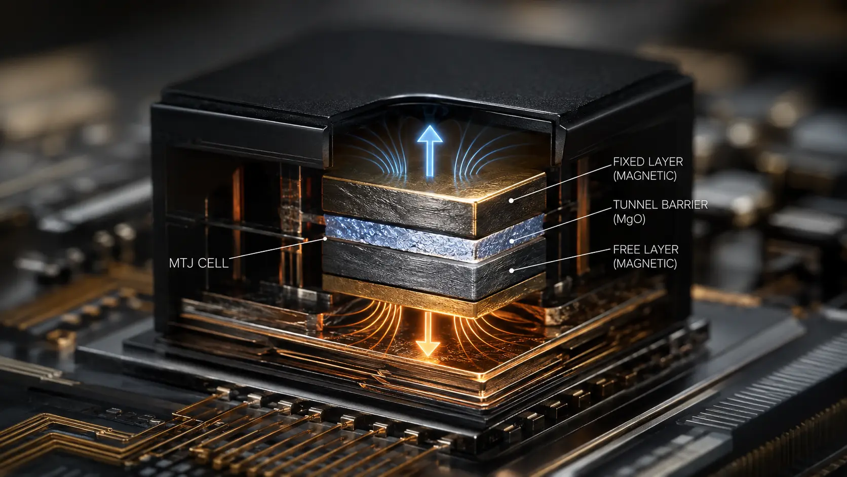
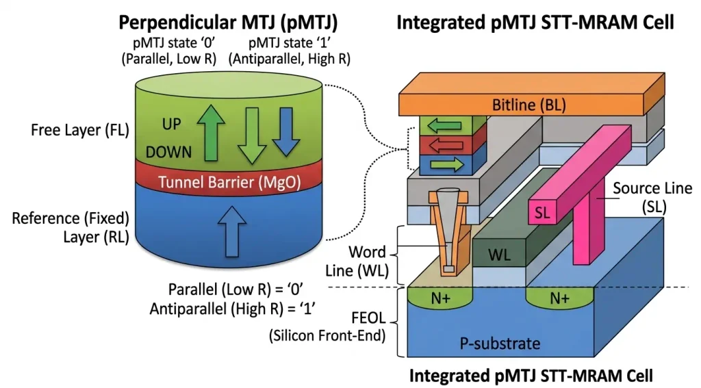
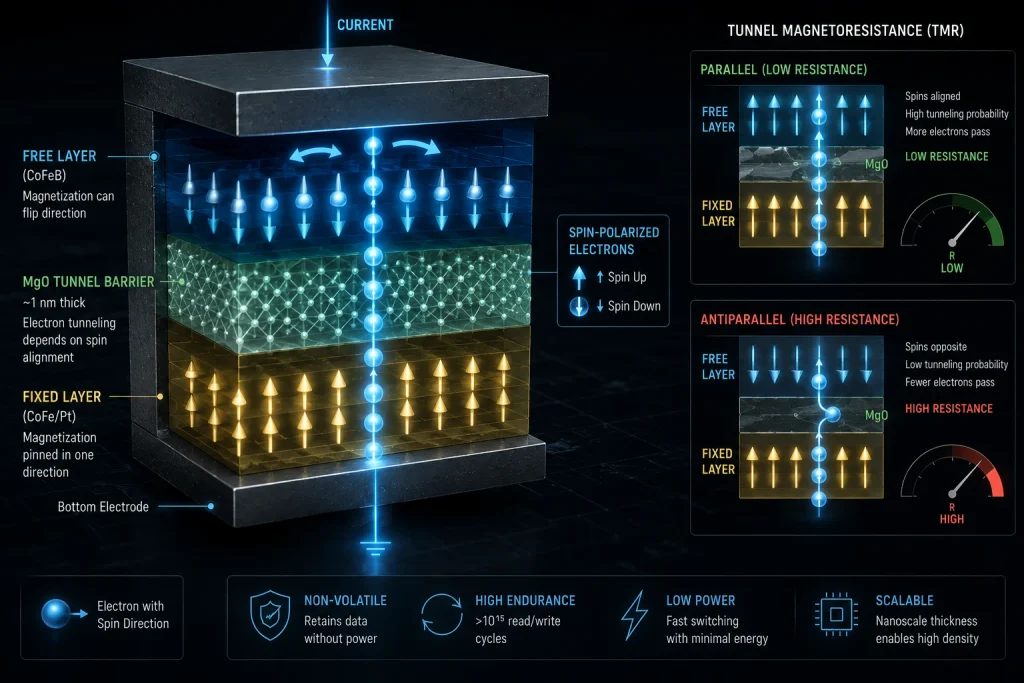
STT-MRAM abandons electrons in favor of a perpendicular Magnetic Tunnel Junction (pMTJ). The pMTJ is a microscopic sandwich consisting of three distinct layers:
- Fixed Layer: A permanent magnet whose magnetic field always points in one direction.
- Tunnel Barrier: An ultra-thin, electrically insulating layer made of Magnesium Oxide (MgO).
- Free Layer: A magnet whose field can be flipped to point either up or down.
3. Technical Depth: Tunnel Magnetoresistance (TMR)
How does the computer read the data? It uses the quantum tunneling effect. When a tiny read current is passed through the sandwich, the resistance changes based on the magnets.
If the Free Layer and Fixed Layer point in the same direction (Parallel), electrons pass easily. The resistance is low, which the computer reads as a digital “0”.
If they point in opposite directions (Anti-Parallel), the electrons struggle to pass. The resistance spikes high, which the computer reads as a digital “1”.
4. Technical Depth: Spin-Transfer Torque (STT)
How do you write data without using a bulky magnetic coil? You use Spin-Transfer Torque.
Every electron acts like a tiny spinning top. Normal electrical current is a chaotic mix of electrons spinning in all directions. When the chip writes data, it pushes the current through a polarizing filter, forcing all the electrons to spin in the exact same direction. When this “spin-polarized” tsunami of electrons slams into the Free Layer, they transfer their angular momentum to the magnetic atoms, physically forcing the Free Layer’s magnetic field to flip over.
5. Real-World Consequences: The Thermodynamic Tradeoff
The stability of the data relies on the Thermal Stability Factor (Δ):
Δ = (Ku * V) / (kB * T)
To survive 150°C (T), engineers must increase the magnetic stiffness (Kᵤ). But if the magnet is too stiff, it requires a massive electrical current to flip during a write operation, which can blast a hole through the fragile MgO barrier and destroy the cell. Automotive STT-MRAM is a masterclass in tuning this exact formula to achieve 10-year retention without sacrificing write endurance.
Automotive Memory Reliability Simulator
eFlash Thermal Degradation vs. STT-MRAM Magnetic Retention
25°C
Ambient (25°C)
AEC-Q100 Grade 0 (150°C)
Commercial Deployments: TSMC and GlobalFoundries
STT-MRAM has crossed the commercial inflection point and is currently fabricated at scale by the world's premier foundries.
TSMC's 22nm Ultra-Low Leakage (ULL) Node: TSMC has actively deployed 22nm STT-MRAM specifically for automotive, IoT, and edge-AI applications. Their process supports -40°C to 150°C operation, completely replacing legacy embedded flash in next-generation microcontrollers. By decoupling the memory from the front-end logic, TSMC allows automotive designers to integrate massive AI processors on the same die as non-volatile memory without thermodynamic compromises.
GlobalFoundries 22FDX eMRAM: GlobalFoundries utilizes their Fully Depleted Silicon-On-Insulator (FD-SOI) architecture paired with STT-MRAM (eMRAM). This combination is fiercely optimized for ultra-low power consumption. For automotive radar and LiDAR systems that must sit behind a car bumper and operate on minimal wattage, the 22FDX eMRAM provides instant-on/instant-off capabilities, writing massive point-cloud datasets instantly without draining the vehicle's electrical grid.
Space and Radiation Hardening: A unique byproduct of relying on magnetic spin instead of electrical charge is radiation immunity. When cosmic rays or high-energy particles hit a standard flash memory cell, they knock the electrons out of place, flipping bits and causing catastrophic software errors (Single-Event Upsets). Because cosmic rays cannot flip a magnetic field, STT-MRAM is intrinsically radiation-hardened. Aerospace firms and satellite manufacturers are actively adopting automotive-grade STT-MRAM for Low Earth Orbit (LEO) avionics.
Economic & Strategic Impact
The core strategic value of STT-MRAM is Lithography Mask Eradication.
In semiconductor manufacturing, every "mask" is a stencil used to print a layer of the chip. eFlash is deeply embedded into the actual silicon at the bottom of the chip, requiring up to 12 expensive, highly complex mask layers to isolate the high-voltage cells from the delicate logic transistors.
STT-MRAM is manufactured in the Back-End-Of-Line (BEOL)—the copper wiring layers sitting high above the silicon. Splicing an MTJ stack between two copper wires requires only 3 or 4 extra masks. This drastically simplifies the manufacturing process, increases wafer yield, and slashes the total production time inside the fab by weeks. The capital expenditure (CapEx) savings heavily outweigh the upfront cost of deploying the new magnetic deposition machines.
Advantages
- AEC-Q100 Grade 0 Compliance: Guaranteed to retain data for 10 years at a continuous 150°C, natively solving the harsh-environment memory crisis for under-the-hood automotive applications.
- Near-Infinite Endurance: While eFlash degrades after 10⁵ cycles, STT-MRAM can theoretically endure > 10¹⁰ write cycles, acting as a flawless, continuous data logger for autonomous vehicle telemetry.
- Byte-Addressability: Flash memory must erase data in massive "blocks" before writing new data, which is brutally slow. STT-MRAM can overwrite single bytes of data instantly, exactly like SRAM or DRAM.
- Instant-On Capability: Because the data is permanent, the chip does not need to waste time booting up and copying software from a hard drive into temporary RAM; the software executes instantly the millisecond the car turns on.
Limitations
- Magnetic Immunity Vulnerabilities: Because the data is magnetic, exposing the chip to an immensely powerful external magnetic field (like an MRI machine or heavy industrial motors) can flip the free layer and erase the data. Automotive MRAM requires careful magnetic shielding in the chip packaging to resist multi-kilo-Oersted stray fields.
- Read Disturb: In STT-MRAM, reading and writing use the exact same physical pathway. To read the data, you pass a small current. To write, you pass a large current. If the read current accidentally spikes due to electrical noise, it can unintentionally flip the magnet, destroying the data during a routine read operation.
- The Endurance vs. Retention Wall: You cannot have infinite retention and infinite endurance simultaneously. If you lock the magnet tightly to survive 150°C heat, you must blast it with higher voltage to write data, which slowly burns through the ultra-thin MgO barrier and kills the cell over time.
Common Misconceptions
Misconception: STT-MRAM has moving parts like an old magnetic hard drive.
Reality: There are absolutely no physical moving parts. The "spin" refers to the quantum angular momentum of electrons. The atoms themselves stay perfectly still; only their invisible magnetic fields flip direction.
Misconception: It will replace the RAM in my gaming PC next year.
Reality: While STT-MRAM is replacing Flash memory, it is still slightly too slow and requires too much write energy to replace the ultra-fast SRAM used in L1/L2 processor caches. It is an embedded storage solution, not a high-bandwidth desktop memory replacement.
Misconception: The chip is magnetic, so it sticks to metal.
Reality: The pMTJ magnets are barely a few nanometers thick. The magnetic forces are strictly contained at the atomic level and exert zero macroscopic pull on the surrounding environment.
What Most People Miss
The disruptive intelligence value of Solder Reflow Survival.
When analysts discuss MRAM, they focus on the car engine. What they miss is the factory floor.
During circuit board manufacturing, chips undergo "solder reflow"—baking in an oven at 260°C to melt the solder and glue them to the board. eFlash is erased at 260°C. Therefore, automakers must solder the empty eFlash chip to the board first, and then waste valuable factory time painstakingly programming the software onto the chip via cables.
STT-MRAM can be engineered to survive six distinct 260°C reflow cycles without dropping a bit. Automakers can pre-program the software onto the STT-MRAM chip at the foundry, ship it, bake it onto the board at 260°C, and put it directly into the car, stripping hours of bottlenecked programming time off the assembly line.
Comparison Table
| Feature | Embedded Flash (eFlash) | SRAM (Cache) | STT-MRAM (Automotive) |
| Data Retention (Power Off) | Yes (Non-Volatile) | No (Volatile) | Yes (Non-Volatile) |
| Write Speed | Microseconds | Sub-Nanosecond | ~30 Nanoseconds |
| Write Endurance | ~10⁵ Cycles | Infinite | ~10¹⁰ Cycles |
| 150°C Heat Tolerance | Poor (Charge leaks) | Moderate | Excellent (Magnetic lock) |
| Mask Layers Required | 10 to 12 (Front-End) | Native to CMOS | 3 to 4 (Back-End) |
Case Study
Situation: The automotive industry’s transition toward Level 3 and Level 4 Advanced Driver Assistance Systems (ADAS) mandated microcontrollers built on advanced sub-28nm silicon nodes. However, these safety-critical systems required embedded non-volatile memory that adhered to rigorous ISO 26262 functional safety standards and AEC-Q100 Grade 1/Grade 0 thermal profiles. Traditional eFlash physically could not scale to 22nm without devastating charge leakage at high temperatures.
Challenge: Qualify a completely new, magnetic embedded memory architecture at 22nm that could survive 150°C continuous operation, resist external magnetic fields, and execute high-speed writes without degrading the dielectric tunnel barrier.
Solution (TSMC's 22nm ULL STT-MRAM): TSMC successfully integrated a pMTJ STT-MRAM stack into their 22nm Ultra-Low Leakage (ULL) CMOS technology. They utilized advanced magnetic shielding in the packaging to provide magnetic immunity exceeding 1100 Oersted at 25°C. To balance the thermodynamic equation, they tuned the perpendicular magnetic anisotropy to favor extreme retention over raw speed.
Outcome: The qualification demonstrated that TSMC's 22nm STT-MRAM achieved zero data loss after six aggressive 260°C solder reflow cycles, and mathematically guaranteed data retention far exceeding 10 years at 150°C. The read operations developed signals in just 6 nanoseconds, while maintaining highly reliable write pulses around 30ns.
Lessons Learned: The deployment validated that leveraging quantum magnetic states in the BEOL is the definitive path forward for automotive silicon. By moving the memory out of the silicon substrate and into the metal layers, the industry successfully decoupled compute scaling from memory physics, securing the ADAS supply chain for the next decade.
Future Outlook
Next 12–24 Months
The era of Widespread Automotive 22nm Adoption. In the immediate term, STT-MRAM will monopolize the design wins for 22nm and 16nm automotive microcontrollers. Tier-1 automotive suppliers (Bosch, Continental) will finalize their transition away from eFlash for all critical engine control units (ECUs) and radar processors. This volume production will rapidly drive down the unit economics of the specialized physical vapor deposition (PVD) machines required to manufacture the MTJ stacks.
Next 3–5 Years
The scaling of Spin-Orbit Torque (SOT-MRAM). The primary limitation of STT-MRAM is that the heavy write current must pass through the fragile MgO barrier, which limits write speed and endurance. The next evolutionary leap is SOT-MRAM. By placing a heavy metal track (like Tungsten or Tantalum) underneath the MTJ, the write current sweeps horizontally beneath the cell rather than punching through it. This decoupling of the read and write paths will allow SOT-MRAM to achieve sub-2-nanosecond write speeds with genuinely infinite endurance, finally positioning magnetic memory to replace SRAM in the L2/L3 processor cache.
Next 10 Years
The Voltage-Controlled (VC-MRAM) Ultimatum. By the mid-2030s, as the world transitions to ultra-dense 3D integration, managing thermal budgets will be the ultimate bottleneck. VC-MRAM will emerge from the laboratory. Instead of using electrical current to flip the magnet (which wastes energy as heat), VC-MRAM uses an electrical voltage field to mathematically alter the magnetic anisotropy, effectively flipping the magnet using near-zero energy. This will drop the power consumption of embedded memory by 99%, establishing the foundation for deeply embedded, zero-power neuromorphic AI architectures.
Most Likely Scenario
STT-MRAM has permanently won the battle to replace embedded Flash. The physics of trapped electrons have mathematically run out of runway. As global foundries standardize the MTJ deposition process, magnetic memory will become a seamless, off-the-shelf IP block for any chip designer. By providing bulletproof, 150°C retention and radiation immunity, STT-MRAM guarantees that the brains driving our autonomous future will never forget their instructions, no matter how harsh the environment becomes.
Key Takeaways
- Legacy embedded Flash (eFlash) memory stores data using trapped electrons. At 150°C inside a car engine, these electrons escape, wiping the memory clean and causing systems to fail.
- Spin-Transfer Torque MRAM (STT-MRAM) solves this by using microscopic magnets instead of electrons. It stores a "1" or "0" based on whether the magnetic field points up or down.
- Because physical magnetic states are highly resistant to heat, STT-MRAM can easily survive 150°C automotive environments for 10 years without losing any data.
- It writes data in nanoseconds (much faster than Flash) and can endure billions of write cycles, making it perfect for real-time data logging and instant Over-The-Air (OTA) updates in self-driving cars.
- Unlike eFlash, which requires complex integration deep inside the silicon, STT-MRAM is built in the copper wiring layers above the chip, saving money and allowing the logic chip to shrink past 28nm.
- The memory is intrinsically immune to cosmic radiation, but it must be carefully shielded in its packaging to ensure strong external magnets do not accidentally erase the data.
Glossary
Back-End-Of-Line (BEOL): The upper layers of a microchip where the copper wiring connects the transistors. STT-MRAM is built here, saving space and complexity in the silicon below.
Magnetic Tunnel Junction (MTJ): A microscopic sandwich of two magnetic layers separated by an ultra-thin insulator. It is the core component that stores the data in an MRAM cell.
Over-The-Air (OTA) Updates: The ability to wirelessly download and install new software into a car's computer. STT-MRAM handles these massive data writes instantly without wearing out.
Solder Reflow: A manufacturing process that uses a 260°C oven to melt solder and glue microchips to a circuit board. STT-MRAM can survive this extreme heat while fully loaded with data.
Spin Polarization: Filtering an electrical current so that all the electrons are spinning in the exact same quantum direction.
Spin-Transfer Torque (STT): The physical mechanism of writing data. A spin-polarized current slams into the free magnetic layer, transferring its momentum and physically flipping the magnet upside down.
Thermal Stability Factor (Δ): The mathematical formula that dictates how strongly the magnet holds its data. High stability means it survives 150°C heat, but requires more energy to overwrite the data.
Sources
TSMC Research: 22nm STT-MRAM for Reflow and Automotive Uses with High Yield
ResearchGate (IEEE): Design Considerations for Optimizing p-MTJ Performance
Synopsys: Future Microcontrollers Need Embedded MRAM (eMRAM)
MDPI Nanomaterials: MRAM: A Versatile Non-Volatile Memory for Next-Generation Cache
Keysight Technologies: Achieve Compliance with ISO 26262 Functional Safety Standards