Advertisement
)

If you want to buy a smartphone with a terabyte of storage today, the memory chips inside cannot simply be made wider. We ran out of flat, horizontal space on microchips a decade ago. To cram more photos, videos, and apps into your pocket, the semiconductor industry started building skyscrapers. Today, a 3D NAND memory chip is a staggering, microscopic metropolis stacked over 300 floors high. But to wire this silicon skyscraper together, engineers must drill “memory holes”—microscopic trenches so deep and narrow that dropping a coin down one is geometrically equivalent to dropping it from the top of the Burj Khalifa to the street below.
Why should you care right now? Because if you try to spray-paint the inside of that trench using standard manufacturing gasses, the top of the hole instantly clogs, leaving the bottom completely bare. The chip fails, and global memory scaling stops. To solve this, the semiconductor supply chain relies entirely on a single, extreme chemical process: Atomic Layer Deposition (ALD). Instead of spraying material, ALD forces precursor gasses to react perfectly, placing exactly one layer of atoms at a time across the entire trench. This microscopic “trench-coating” technology is the absolute bottleneck governing the future of the multi-billion-dollar global memory market.
What is Atomic Layer Deposition (ALD)?
Atomic Layer Deposition (ALD) is a highly precise chemical manufacturing process used in semiconductor fabrication. It utilizes alternating pulses of reactive precursor gasses to deposit ultra-thin, perfectly uniform films onto a microchip. Because the chemical reactions are self-limiting, ALD builds material exactly one atomic layer at a time, ensuring perfect coverage inside microscopic, high-aspect-ratio trenches.
At a Glance
- Concept: Coating the inside of a microscopic hole by using two separate gasses that lock together like puzzle pieces, but only one layer at a time.
- Why it matters: As memory chips are stacked 300 to 400 layers high, the trenches drilled through them become incredibly deep and narrow. Traditional coating methods clog the top of the hole. ALD guarantees the bottom gets coated perfectly.
- Who uses it: Mega-foundries (TSMC, Intel), memory giants (Samsung, Micron, SK Hynix), and the semiconductor equipment monopolies that build the ALD machines (ASM International, Applied Materials).
- Biggest takeaway: ALD is flawless, but it is agonizingly slow. Building a film thick enough to act as an insulator might require repeating the exact same gas-pulse cycle thousands of times per wafer, creating a massive traffic jam in the factory.
In Simple Words
Imagine you have a long, incredibly narrow glass tube, and you need to paint the entire inside perfectly red.
If you use Chemical Vapor Deposition (CVD), you take a can of red spray paint and blast it down the tube. The paint covers the opening instantly, builds up too fast, and clogs the top. The middle and bottom of the tube never get any paint at all.
If you use Atomic Layer Deposition (ALD), you use chemistry instead of brute force.
First, you pump an invisible “blue” gas into the tube. The blue gas is sticky, but it cannot stick to itself. It coats the entire inside wall with exactly one layer of blue molecules and then stops. You flush the extra blue gas out with air.
Next, you pump in a “yellow” gas. The yellow gas only sticks to blue gas. It attaches perfectly to the blue layer, instantly turning it red, but again, it won’t stick to itself.
By repeating this cycle—blue gas, flush, yellow gas, flush—you build up the red paint exactly one atomic layer at a time. It is impossible to clog the top because the gasses naturally stop reacting once the surface is full, ensuring the bottom of the tube is painted just as perfectly as the top.
Why This Matters
For Semiconductor Engineers, Hardware VCs, and Supply Chain Analysts, ALD is the absolute governor of capital expenditure (CapEx) in a fabrication plant (fab).
Because ALD is a cycle-based process, it is inherently slow. A modern 300-layer 3D NAND wafer might spend hours inside an ALD chamber just to deposit a few nanometers of dielectric film. As layer counts increase, the number of ALD machines a factory must purchase to maintain its output (Wafers Per Hour) skyrockets. A fab that previously needed 20 deposition tools now needs 60. This dynamic shifts billions of dollars of revenue directly to ALD equipment manufacturers (like ASM International and Lam Research), making atomic-level chemistry the single most critical choke point in the economics of global data storage.
The Aspect Ratio Crisis in 3D NAND
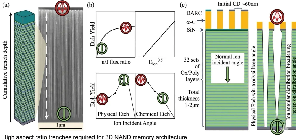
The evolution of microchips is a war against aspect ratios.
In early 2D chips, transistors were flat. Coating them was like painting a parking lot—easy and fast. But the shift to 3D NAND architectures required drilling “memory holes” straight down through hundreds of alternating layers of material. Today, these holes have an aspect ratio greater than 100:1 (meaning they are 100 times deeper than they are wide). In the future 500-layer era, they will push past 200:1. At these dimensions, standard physics fail. The only way to maneuver material down a 200:1 microscopic canyon is to rely on the self-limiting thermodynamics of ALD.
How Atomic Layer Deposition (ALD) Works
Coating a trench with 100% conformality without causing a “pinch-off” requires perfectly orchestrated, sequential chemistry. Here is the first-principles breakdown of the architecture.
1. The Fundamental Problem: Line-of-Sight and Pinch-Off
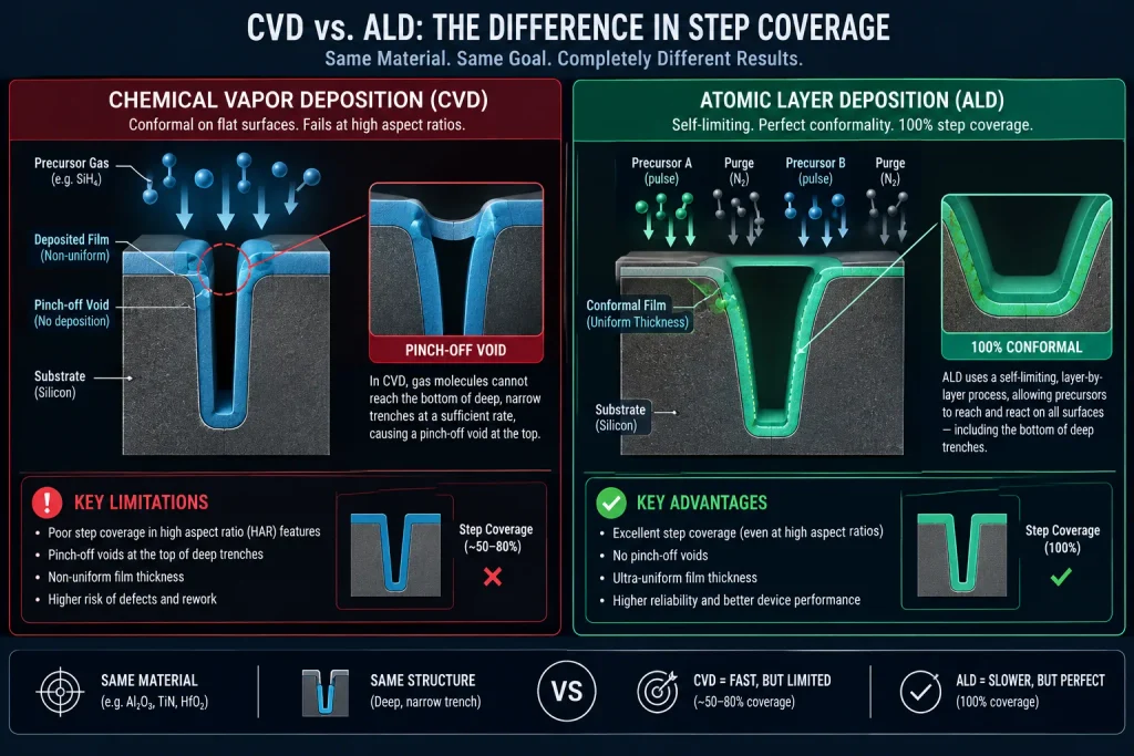
In standard physical (PVD) or chemical (CVD) deposition, material is continuously blasted at the wafer. Because the material molecules are reacting with each other in the air before they hit the surface, they pile up at the very first surface they touch—the opening of the trench. This creates an “overhang” that eventually pinches off and seals the top of the trench entirely, leaving a fatal, empty void at the bottom.
2. The Core Mechanism: Self-Limiting Half-Reactions
ALD bypasses this by completely separating the chemicals. The process relies on two distinct precursor gasses (Precursor A and Precursor B) that are never allowed in the chamber at the same time.
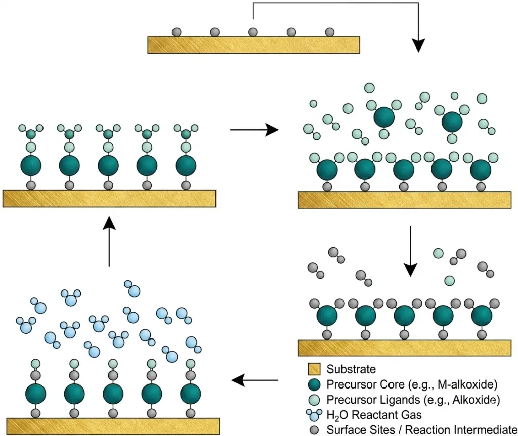
3. Technical Depth: The 4-Step ALD Cycle
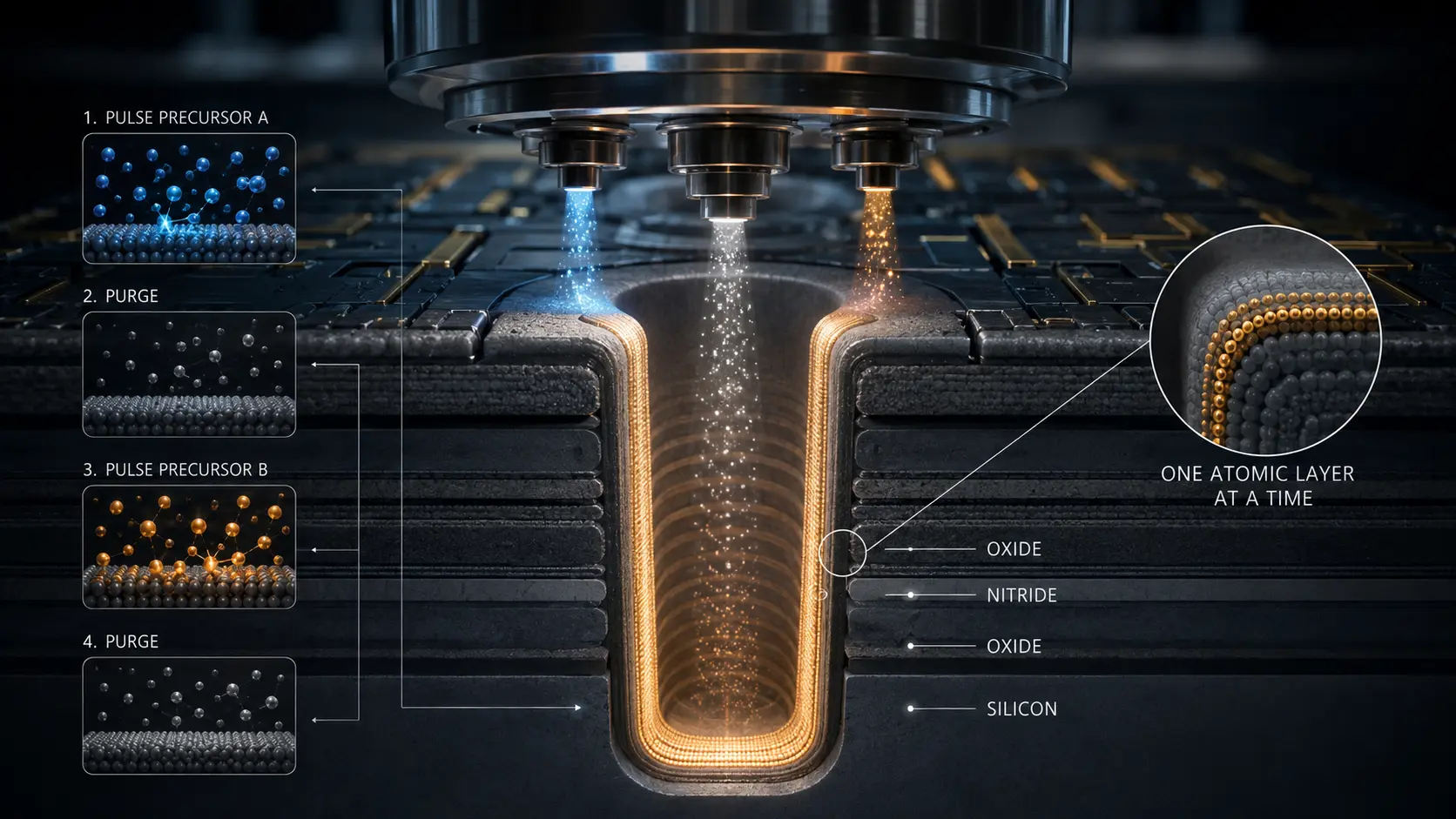
To deposit a common insulator like Aluminum Oxide (Al₂O₃), the tool executes a precise loop:
- Pulse Precursor A: Trimethylaluminum (TMA) gas is pumped into the chamber. It bonds with the hydroxyl groups on the bare silicon surface. Crucially, TMA molecules will not bond to other TMA molecules. Once the surface is covered by a single monolayer of TMA, the reaction naturally stops (it is “self-limiting”).
- Purge: An inert gas (like Nitrogen) sweeps all the leftover, unreacted TMA out of the chamber.
- Pulse Precursor B: Water vapor (H₂O) is introduced. The water chemically reacts exclusively with the TMA layer, stripping away the methyl groups and leaving behind a pristine, solid atomic layer of Al₂O₃.
- Purge: The leftover water and reaction byproducts (methane) are swept out.
This single four-step cycle deposits roughly 0.1 nanometers of material. To build a 10-nanometer film, the machine must repeat this exact loop 100 times.
4. Real-World Consequences: Perfect Conformality
Because the reaction stops itself once the surface is full, Precursor A has time to drift all the way down to the absolute bottom of the 100:1 trench before the purge happens. The resulting film follows the exact geometric contours of the hole with 100% uniformity. Whether it is at the top rim or the deep floor, the coating is exactly the same thickness.
ALD Applications: 3D NAND and DRAM High-k Capacitors
The theoretical perfection of ALD is the absolute bedrock of modern high-density data storage.
3D NAND Charge Trap Layers: In 3D NAND, data is stored by trapping electrons inside a microscopic layer of silicon nitride that lines the wall of the memory hole. If this insulating layer is even one nanometer too thick at the top and too thin at the bottom, the electrical voltage required to read the data will be completely mismatched, corrupting the memory block. ALD is the only way to line the 300-layer hole with a charge trap layer that is mathematically identical from top to bottom.
DRAM High-k Capacitors: While 3D NAND relies on deep trenches, Dynamic Random Access Memory (DRAM) relies on incredibly tall, microscopic pillars (capacitors) to hold electrical charge. To prevent the charge from leaking out of the pillars, they must be coated in “High-k” dielectric materials (like Hafnium Oxide). As DRAM nodes shrink below 12 nanometers, these pillars are placed so close together that they almost touch. Only ALD can slide between the pillars and wrap them in a flawless insulating shield.
Multi-Patterning Lithography (SADP/SAQP): When EUV lithography machines cannot print lines fine enough, engineers use a trick called Self-Aligned Double Patterning (SADP). They use a laser to print a standard block, and then use ALD to grow a perfectly precise, 2-nanometer “spacer” wall against the side of the block. They then dissolve the original block, leaving only the ultra-thin ALD walls behind to act as the new, microscopic circuit wires.
Economic & Strategic Impact
The core strategic vulnerability of ALD is the Throughput-to-CapEx Ratio.
In semiconductor manufacturing, time is money. A standard CVD machine blasts gas continuously and can coat a wafer in seconds. ALD requires valves to physically open and close thousands of times to pulse and purge the gasses.
If a 300-layer 3D NAND chip requires a 15-nanometer film, the ALD tool might need 150 cycles. If each cycle takes 5 seconds, that wafer is trapped inside the machine for over 12 minutes. For a mega-fab producing 100,000 wafers a month, a 12-minute traffic jam is financially catastrophic. To solve this, fabs are forced to purchase massive, highly expensive “Batch ALD” furnaces that can process 150 wafers simultaneously, funneling billions of dollars into the capital equipment monopolies that control the ALD patent landscape.
Advantages
- 100% Conformal Step Coverage: Perfectly coats extreme 3D geometries (canyons, pillars, and overhangs) with zero variations in thickness.
- Absolute Thickness Control: Because growth is controlled precisely by the number of chemical cycles (e.g., exactly 0.1 nm per cycle), engineers can dial in the exact atomic thickness of the film mathematically.
- Low-Temperature Viability: Certain advanced ALD processes (like Plasma-Enhanced ALD) can deposit robust films at relatively low temperatures (under 400°C), protecting delicate underlying copper wiring from melting in the Back-End-Of-Line (BEOL).
- Pinhole-Free: The self-limiting reaction ensures that every single microscopic gap on the surface is filled, creating a dense, flawless barrier against electrical leakage.
Limitations
- Extreme Slowness: The sequential nature of the gas pulses and purges makes ALD the slowest deposition method in the fabrication plant.
- Steric Hindrance: Some precursor gas molecules are physically bulky. When they latch onto the surface, their large “arms” physically block adjacent binding sites. This means a single pulse might only achieve 30% coverage of a layer, forcing the cycle to be repeated multiple times just to finish a single atomic plane.
- Precursor Volatility: The gasses used in ALD must be highly reactive, making them toxic, expensive, and unstable. Managing the supply chain for complex organometallic precursors (like Hafnium or Ruthenium) requires immense safety infrastructure.
Common Misconceptions
Misconception: ALD lays down a solid, unbroken blanket of atoms in one pulse.
Reality: Because of “steric hindrance” (the molecules being too bulky), a single pulse of Precursor A might only cover a fraction of the surface. It is a messy, statistical process that relies on multiple cycles to eventually fill in all the gaps and form a solid layer.
Misconception: The gasses mix inside the chamber to create the coating.
Reality: If the gasses ever mix in the chamber air, the process is ruined (it becomes CVD). The entire magic of ALD is that the gasses are strictly separated by inert nitrogen purges so they can only react with the surface of the wafer.
Misconception: ALD is only used for microchips.
Reality: While famous for semiconductors, ALD is actively used to coat OLED flexible displays to protect them from moisture, to coat lithium-ion battery powders to prevent degradation, and to anti-reflectively coat solar panels.
What Most People Miss
The disruptive intelligence value of Spatial ALD.
Most analysts view the slowness of “Temporal ALD” (waiting for the chamber to fill, purge, fill, and purge) as a permanent law of physics. What they miss is the mechanical workaround: Spatial ALD.
Instead of sitting still in a chamber while the gasses change over time, Spatial ALD moves the wafer through space. The machine has a continuous “curtain” of Precursor A gas, followed by a curtain of Nitrogen, followed by a curtain of Precursor B. The silicon wafer is placed on a high-speed rotating platter that simply spins it rapidly through the gas curtains. By swapping time for physical movement, Spatial ALD effectively transforms the sequential, slow ALD chemistry into a continuous, high-throughput manufacturing engine, rescuing the economics of the fabrication plant.
Comparison Table
| Feature | Physical Vapor Deposition (PVD) | Chemical Vapor Deposition (CVD) | Atomic Layer Deposition (ALD) |
| Deposition Method | Sputtering solid metal | Continuous gas phase reaction | Sequential self-limiting gas pulses |
| Speed / Throughput | Very Fast | Fast | Very Slow |
| Step Coverage | Poor (Line-of-sight only) | Moderate (Prone to pinch-off) | Perfect (100% Conformal) |
| High Aspect Ratios | Fails | Fails at extreme depths | Excels (>100:1 trenches) |
| Thickness Control | Moderate | Good | Absolute (Atomic level precision) |
Case Study
Situation: As consumer demand for massive data storage surged, memory manufacturers like Samsung, SK Hynix, and Micron recognized that 2D planar NAND had reached its physical scaling limit. They pivoted to 3D NAND, stacking memory cells vertically. By the time they reached 176 and 232 layers, the memory hole trenches became astoundingly deep, boasting aspect ratios exceeding 60:1.
Challenge: To trap electrical charge and store data, the inside of these deep memory holes had to be lined with an ultra-thin stack of ONO (Oxide-Nitride-Oxide) dielectric films. When manufacturers attempted to use legacy CVD tools, the gasses clogged the top of the 232-layer trench, leaving the bottom cells un-coated and destroying the memory yield.
Solution (The Transition to High-k ALD): The mega-fabs completely overhauled their deposition lines, adopting advanced Batch ALD furnaces provided by equipment leaders like ASM International and Tokyo Electron (TEL). They utilized precise precursors to pulse atomic layers of dielectric material down into the deep trenches.
Outcome: The ALD chemistry bypassed the line-of-sight and diffusion limits of CVD. The precursors drifted to the absolute bottom of the 200+ layer trenches, attached to the silicon wall, and self-terminated perfectly. This allowed the memory giants to successfully yield 232-layer and eventually 300-layer 3D NAND architectures, keeping the global cost-per-gigabyte of solid-state drives (SSDs) on a downward trajectory.
Lessons Learned: The 3D NAND transition proved that Moore’s Law is no longer strictly about lithography (printing smaller lines); it is fundamentally about 3D materials engineering. The ability to manipulate chemistry one atomic layer at a time inside deep vertical structures is the true engine sustaining the global memory market.
Future Outlook
Next 12–24 Months
The era of Plasma-Enhanced ALD (PEALD) in the BEOL. In the immediate term, the industry will focus on the upper wiring layers of the chip (Back-End-Of-Line). Because the delicate copper wires in these upper layers melt at high temperatures, standard thermal ALD cannot be used. Foundries will heavily deploy Plasma-Enhanced ALD. By striking the precursor gasses with an RF plasma, the gasses become hyper-reactive, allowing the ALD process to occur at incredibly low temperatures (under 300°C), protecting the copper while still depositing flawless insulating barriers.
Next 3–5 Years
The scaling of Area-Selective ALD (AS-ALD). Currently, ALD coats the entire wafer blindly. Engineers then have to use expensive lithography and etching tools to carve away the parts they don’t want. The next major leap is Area-Selective ALD. By pre-treating the wafer with specific chemical “inhibitors,” engineers can instruct the ALD gas to only stick to the metallic wires and completely ignore the silicon insulators. This “bottom-up” 3D printing bypasses traditional lithography entirely, saving the fab billions of dollars in etching equipment and alignment errors.
Next 10 Years
The 500-Layer 3D NAND Barrier. As manufacturers push toward 400-layer and 500-layer 3D NAND chips, the memory hole aspect ratios will approach an absurd 200:1 or 300:1. At these depths, even standard ALD precursors struggle to physically diffuse all the way to the bottom before the purge cycle kicks in. The industry will be forced into a “multi-tier” approach—drilling a 250-layer hole, coating it with ALD, gluing a second 250-layer block on top, and drilling again. The foundries that master the precise alignment and ALD bonding of these multi-tier mega-structures will dictate the baseline economics of cloud storage for the 2030s.
Most Likely Scenario
Atomic Layer Deposition guarantees the survival of 3D chip architectures. As microchips transition from flat cities into vertical skyscrapers, the ability to control matter at the atomic level dictates success. While its inherent slowness will always be a supply chain bottleneck, the brute-force deployment of massive ALD batch furnaces and Spatial ALD rotators ensures that the semiconductor industry can continue to cram more data into microscopic trenches, sustaining the hardware requirements of the artificial intelligence boom.
Key Takeaways
- To increase storage capacity, modern memory chips are stacked over 300 layers high, requiring engineers to drill microscopic trenches straight down through the layers.
- Standard coating methods (like spraying gas) fail because the material clogs the top of the deep trench, leaving the bottom completely bare.
- Atomic Layer Deposition (ALD) solves this using self-limiting chemistry. It pulses two gasses one at a time. The first gas coats the wall and naturally stops sticking once the surface is full.
- Because the reaction stops itself, the gas has time to travel to the absolute bottom of the trench, ensuring the coating is perfectly even from top to bottom.
- ALD builds material exactly one atom layer at a time, making it incredibly precise but agonizingly slow, creating a massive operational bottleneck in semiconductor factories.
- To speed up the process, fabs are investing heavily in “Spatial ALD,” which moves the chip rapidly through continuous curtains of gas rather than waiting for a chamber to fill and empty.
Glossary
Aspect Ratio: The ratio of a trench’s depth to its width. A memory hole in 3D NAND can have an aspect ratio of 100:1, making it incredibly difficult to coat the inside walls.
Batch ALD: A massive industrial furnace that performs the slow ALD cycle on 100 to 150 wafers simultaneously, offsetting the slowness of the process with massive volume.
Chemical Vapor Deposition (CVD): A continuous gas process that is faster than ALD but prone to “pinch-off” errors in deep trenches because the gasses react continuously in the air.
Conformal Coating: A film that perfectly follows the exact 3D shape of the surface it is applied to, maintaining exactly the same thickness on flat plains, vertical walls, and deep corners.
Precursor Gas: The specific, highly reactive chemicals (like Trimethylaluminum or water vapor) that are pulsed into the ALD chamber to create the coating.
Self-Limiting Reaction: A chemical reaction that naturally stops itself once the available surface area is completely covered, preventing the material from piling up or clogging.
Sources
ASM International: Atomic Layer Deposition (ALD) Technology and Solutions
Applied Materials: Engineering 3D NAND Memory Holes with ALD
Journal of Vacuum Science & Technology: Atomic layer deposition: An overview of basic chemistry and applications
Semiconductor Engineering: The Challenges of 300-Layer 3D NAND and Aspect Ratios
Imec: Area-selective atomic layer deposition (AS-ALD) for next-generation nanoelectronics