Advertisement
)

A modern extreme ultraviolet (EUV) lithography machine is the most complex device ever manufactured by humans. It fires a high-powered laser at a microscopic droplet of liquid tin 50,000 times a second, generating a plasma as hot as the surface of the sun. This plasma emits a microscopic beam of 13.5-nanometer light used to carve the billions of transistors inside your smartphone. However, this light is so fragile that even the ambient oxygen in the air absorbs it. To print the chip, the machine must operate in a hard vacuum. But there is a fatal flaw in this environment: dust. If a single microscopic particle lands on the $30 million “photomask” blueprint during printing, every single microchip produced will be defective.
Why should you care right now? Because the standard solution—covering the blueprint with a protective plastic or polysilicon film—no longer works. As chipmakers push these machines to unprecedented 400-watt power levels to print sub-2-nanometer chips, the extreme heat instantly vaporizes standard protective films. To prevent the global semiconductor roadmap from stalling, scientists have turned to one of the most exotic materials in the universe. By spinning a free-standing, atom-thick web of pure Carbon Nanotubes (CNTs), engineers have created a protective shield that survives 1,000°C temperatures while remaining 95% invisible to extreme light, officially securing the next decade of advanced computing.
What are Carbon Nanotube (CNT) EUV Pellicles?
Carbon Nanotube (CNT) EUV pellicles are ultra-thin, free-standing protective membranes used in Extreme Ultraviolet (EUV) lithography scanners. Spun from a mesh of single-walled carbon nanotubes, they protect expensive photomasks from microscopic dust particles while enduring 400-watt laser powers and maintaining over 90% transmittance for 13.5-nanometer light.
At a Glance
- Concept: Wrapping a multi-million-dollar microchip stencil in a microscopic “Saran wrap” made of pure carbon to keep it perfectly clean during the manufacturing process.
- Why it matters: Older protective films melt when hit by the massive 400W lasers required to make the next generation of artificial intelligence chips. CNTs do not melt.
- Who uses it: Global semiconductor foundries (TSMC, Intel, Samsung), photolithography equipment monopolies (ASML), and elite nano-materials research institutes (Imec).
- Biggest takeaway: A CNT pellicle isn’t a solid sheet of material; it is a highly porous, chaotic web. Because it is mostly empty space, the fragile EUV light passes straight through it without being absorbed or distorted.
In Simple Words
Imagine you are using a very expensive, irreplaceable glass stencil to spray-paint a masterpiece.
To protect the glass stencil from getting dirty, you cover it in a layer of clear Saran wrap. The paint goes through the holes in the stencil, and any random dust in the room falls on the Saran wrap instead of ruining your expensive glass. This is how a pellicle works.
However, in advanced microchip manufacturing, the “spray paint” is a laser beam so powerful it acts like a blowtorch. When you turn the blowtorch on, the standard Saran wrap (polysilicon) instantly melts and catches fire.
A Carbon Nanotube (CNT) Pellicle is a piece of Saran wrap made out of an almost indestructible, invisible titanium mesh. It is so thin that the light passes right through it, but it is so thermodynamically resilient that the blowtorch doesn’t even leave a mark. It protects the stencil perfectly without melting.
Why This Matters
For Semiconductor Engineers, Photolithography Specialists, and Hardware VCs, the CNT pellicle solves the “Throughput vs. Yield” paradox of High-NA EUV.
At $350 million per machine, an ASML High-NA scanner must print well over 150 wafers per hour to be economically viable. To reach this throughput, the EUV source power must be cranked to 400W, 500W, or even 600W. If a foundry operates without a pellicle to avoid melting it, they suffer catastrophic yield losses from dust “fall-on” defects. If they use a legacy polysilicon pellicle, they are forced to throttle the laser down to 250W, destroying the machine’s financial throughput. CNT pellicles are the only known material science capable of breaking this deadlock, enabling foundries to run their machines at maximum wattage with zero dust defects.
The Evolution of EUV Lithography Pellicles
The evolution of the pellicle mirrors the transition from Deep Ultraviolet (DUV) to Extreme Ultraviolet (EUV).
In the DUV era, light was bounced through the mask using 193-nanometer lasers. Because 193nm light easily passes through solid matter, pellicles were thick, cheap, and made of simple fluoropolymers (Teflon-like plastics).
When the industry shifted to 13.5nm EUV light, the physics broke. 13.5nm light is ionizing radiation; it is absorbed by literally everything, including air. Plastics turned black and shattered instantly. The industry was forced into a decade-long crisis, attempting to engineer ultra-thin polysilicon membranes that were fragile, brittle, and absorbed 15% of the light. The shift to Carbon Nanotubes abandons solid films entirely, moving the industry into the realm of structured, porous nano-meshes.
How Carbon Nanotube (CNT) Pellicles Work
Surviving the focal plane of an EUV scanner requires bending the laws of thermodynamics and optical transparency. Here is the first-principles breakdown of the architecture.
1. The Fundamental Problem: Sub-Wavelength Absorption
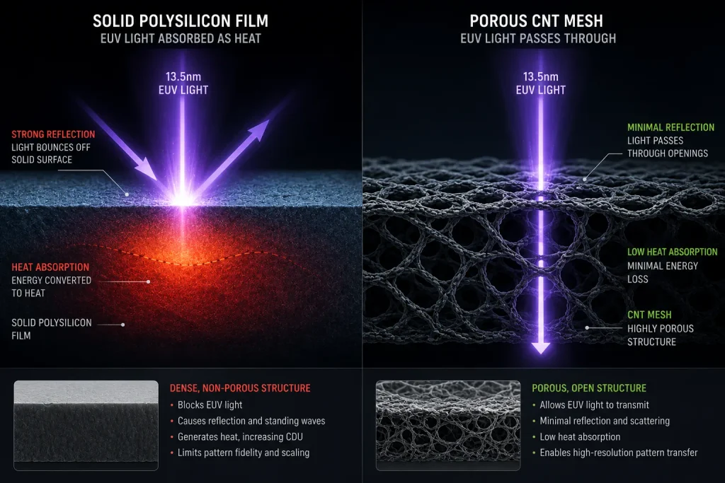
When an EUV photon strikes a pellicle, it either transmits through, reflects, or gets absorbed. Absorbed photons transfer their kinetic energy into the membrane as heat. Because 13.5nm light is highly absorbable, standard membranes heat up violently. In a vacuum chamber, there is no air to carry this heat away via convection.
2. The Core Mechanism: The Porous Carbon Network
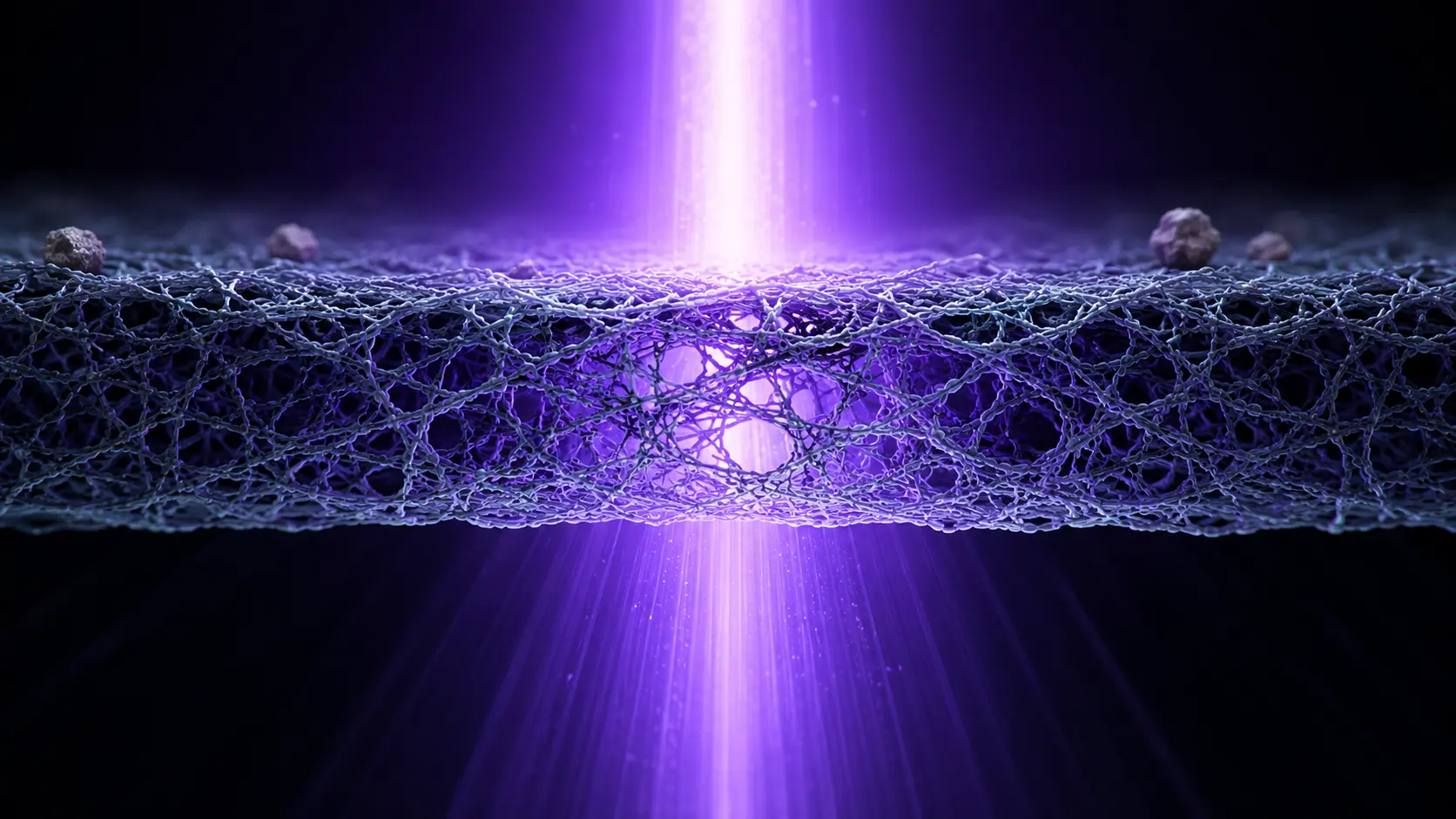
A CNT pellicle is not a solid sheet. It is a non-woven, chaotic network of Single-Walled Carbon Nanotubes (SWCNTs).
These tubes are only 1.5 to 2 nanometers in diameter. Because the network is highly porous (mostly empty space), it physically interacts with fewer photons. This porosity allows the membrane to achieve an EUV transmittance of 95%, meaning only 5% of the 400-watt laser beam is actually absorbed as heat.
3. Technical Depth: Radiative Cooling and Emissivity
Despite the high transmittance, absorbing 5% of a 400W laser in a vacuum still generates intense heat. Because there is no air for convective cooling, the membrane must rely entirely on radiative cooling, governed by the Stefan-Boltzmann law:
P = εσAT⁴
Carbon nanotubes possess an exceptionally high thermal emissivity (ε ≈ 0.9). As the laser strikes the pellicle, the CNTs instantly radiate the thermal energy away as infrared heat. The sp² hybridized carbon bonds are so strong that the mesh can routinely survive temperatures exceeding 1,000°C without oxidizing or melting.
4. Bypassing Mechanical Resonance
Inside the ASML scanner, the vacuum chamber undergoes violent “pump-down” and “venting” cycles, causing massive, rapid pressure fluctuations. Brittle polysilicon pellicles frequently snap under this acoustic stress. CNTs are highly elastic and possess a massive Young’s modulus (tensile strength). They act like a microscopic trampoline, stretching and rebounding during pressure cycles without tearing.
5. Real-World Consequences: Out-of-Focus Defect Mitigation
The pellicle is mounted a few millimeters above the actual photomask. If a dust particle falls on the pellicle, it is held outside the focal plane of the laser. The laser light bends around the dust particle, ensuring that its shadow is completely blurred and undetectable by the time the light hits the silicon wafer, preserving a flawless transistor print.
High-NA EUV Commercial Deployments
The integration of CNT pellicles is moving rapidly from the laboratory to the apex of global semiconductor manufacturing.
ASML High-NA (EXE:5000) Deployments: The newest generation of extreme ultraviolet lithography (High-NA) uses vastly larger optical lenses to print transistors down to 1.4 nanometers. These optics drastically increase the intensity of the light hitting the reticle. Standard pellicles are mathematically disqualified for these tools. Foundries like TSMC and Intel are aggressively collaborating with pellicle suppliers to ensure CNT membranes are qualified in time for High-NA volume production in 2026/2027.
Logic vs. Memory Foundries: The economics of pellicles dictate their use cases. In logic foundries (making CPUs/GPUs for Apple or Nvidia), the photomask prints highly complex, unrepeatable patterns. A single dust defect destroys the whole processor, making CNT pellicles mandatory. In contrast, memory foundries (making DRAM) print highly repetitive grid structures and have built-in redundancy, allowing them to tolerate some dust. However, as memory margins tighten and layer counts increase, even memory giants like Samsung are evaluating CNT pellicles to push yields toward 99%.
EUV Mask Inspection Systems: Before a photomask is loaded into the scanner, it must be inspected for flaws using an actinic (13.5nm) inspection tool. Because CNT pellicles have over 95% transmittance, the inspection laser can see through the pellicle cleanly to inspect the mask underneath without removing the protective cover, drastically reducing the handling time and contamination risk in the cleanroom.
Economic & Strategic Impact
The core strategic value of the CNT pellicle is the optimization of the Wafers Per Hour (WPH) Equation.
A leading-edge semiconductor fab costs over $25 billion to build. The financial model of the fab relies entirely on pushing maximum wafers through the bottleneck tools (the EUV scanners).
If a polysilicon pellicle limits the laser to 250W, the machine might only print 100 wafers per hour. By upgrading to a CNT pellicle that allows a 400W laser, the machine can print 160 wafers per hour. Across a fleet of 20 scanners running 24/7, that 60% increase in throughput equates to billions of dollars in highly profitable, additional silicon logic generated per year, paying for the complex R&D of the CNT pellicle millions of times over.
Advantages
- Extreme Thermal Tolerance: Employs high thermal emissivity to radiate heat instantly in a vacuum, surviving laser source powers up to 600W without melting, shrinking, or sagging.
- High Optical Transmittance: The highly porous, non-woven carbon mesh allows over 95% of 13.5nm EUV light to pass through, reducing the amount of laser power wasted during the printing process.
- Acoustic & Mechanical Resilience: Single-walled carbon nanotubes possess immense tensile strength. The membrane acts like a flexible net, easily surviving the violent air-pressure changes that shatter brittle silicon films.
- Chemical Stability: Pure carbon networks do not outgas toxic chemicals under intense radiation, preventing a hazy film from forming on the expensive internal mirrors of the ASML scanner.
Limitations
- Manufacturing Defect Rates: Spinning a perfectly uniform network of carbon nanotubes across a massive 110mm x 140mm frame is incredibly difficult. If the nanotubes randomly clump together into a “bundle,” that thick bundle blocks the EUV light and casts a lethal shadow on the microchip.
- Hydrogen Radical Etching: Inside the EUV scanner, the laser turns trace amounts of hydrogen gas into highly reactive hydrogen radicals. These radicals aggressively attack and “etch” pure carbon. To survive, the CNTs must be carefully coated in ultra-thin protective layers (like Ruthenium), which adds manufacturing complexity and slightly lowers optical transmittance.
- Inspection Visibility: Standard cleanroom lasers use UV light to check the pellicle for dust. Because CNTs are visually dark and absorb regular UV light, standard inspection tools cannot easily see the dust resting on top of them, forcing foundries to buy new, highly expensive inspection machinery.
Common Misconceptions
Misconception: The pellicle touches the microchip.
Reality: The pellicle never touches the microchip (the wafer). It sits a few millimeters above the photomask (the glass stencil at the top of the machine), protecting the blueprint, not the product.
Misconception: The pellicle is a solid, glass-like sheet.
Reality: A CNT pellicle is a highly chaotic, non-woven mesh that resembles a microscopic chain-link fence or a spiderweb. It is mostly empty space.
Misconception: Dust on the pellicle stops the laser from working.
Reality: The physics of optics handles the dust. Because the pellicle is held a few millimeters away from the focal plane of the blueprint, any dust resting on the pellicle is completely out of focus. The massive laser beam simply bends around the microscopic speck of dust, leaving no shadow on the actual silicon.
What Most People Miss
The disruptive intelligence value of Actinic Transmittance Scaling.
Most analysts assume a pellicle is just a static cost. What they miss is how the transmittance percentage radically alters the compounding geometry of the fab.
Because light passes through the pellicle twice (once on the way to the reflective mask, and once bouncing off the mask toward the wafer), the math compounds. A legacy 85% transmissive pellicle results in a total system transmission of only 72% (0.85 × 0.85. A CNT pellicle with 95% transmittance yields 90% total system transmission (0.95 × 0.95). By rescuing 18% of the lost laser light, foundries can drastically reduce the electrical consumption of the megawatt lasers, lowering the massive energy footprint of the fabrication plant.
Comparison Table
| Feature | Polysilicon (pSi) Pellicle | Silicon Nitride (SiN) Composite | Carbon Nanotube (CNT) Pellicle |
| Material Structure | Solid crystalline film | Solid composite film | Porous, non-woven mesh |
| EUV Transmittance | ~85% | ~90% | > 95% |
| Max Source Power | ~250 Watts | ~300 Watts | 600+ Watts |
| Thermal Emissivity | Low (Melts easily) | Moderate | Extremely High (~0.9) |
| Mechanical Strength | Highly brittle | Moderate | Highly elastic (Trampoline effect) |
| Primary Use Case | Low-Volume N7/N5 Nodes | Standard EUV (N3) | High-NA EUV (N2 / A14) |
Case Study
Situation: As global foundries advanced to the 2-nanometer (N2) node, the necessity of High-NA EUV scanners became absolute. However, running these scanners at the required 400W source power was physically destroying standard polysilicon pellicles. The membranes were absorbing too much heat, sagging into the focal plane, and eventually fracturing, showering the $30 million photomasks with catastrophic debris.
Challenge: Develop a pellicle membrane capable of surviving 400W+ thermal loads in a vacuum, enduring 10,000 Pa/sec acoustic pressure drops, and achieving >95% transmittance, all while remaining chemically stable against hydrogen radical etching.
Solution (The Imec & ASML CNT Initiative): The premier semiconductor research institute, Imec, in collaboration with ASML and global materials suppliers, spearheaded the development of full-reticle-size Carbon Nanotube pellicles. They successfully engineered a technique to spin single-walled CNTs into a highly porous network. To combat the hydrogen etching environment inside the scanner, the team developed a proprietary, ultra-thin multi-layer coating (utilizing transition metals) to shield the carbon mesh without sacrificing optical transparency.
Outcome: In extensive testing environments simulating 400W to 600W laser exposure, the coated CNT pellicles demonstrated absolute thermal resilience, leveraging their high emissivity to radiate heat instantly. The membranes survived rigorous 10,000 pump-vent vacuum cycles without tearing. As of 2025/2026, the technology exited the laboratory, with major suppliers preparing for High-Volume Manufacturing (HVM) to support the rollout of Intel and TSMC’s sub-2nm commercial nodes.
Lessons Learned: The advancement proved that extending Moore’s Law relies as much on materials science as it does on optics. By shifting from solid films to porous, nanostructured meshes, the industry resolved the thermodynamic bottleneck of EUV lithography, ensuring that the extreme power levels required for next-generation logic chips could be harnessed safely and economically.
Future Outlook
Next 12–24 Months
The era of HVM Defect Yield Optimization. In the immediate term, the industry’s singular focus will be on the manufacturing yield of the pellicles themselves. Producing a 110mm x 140mm sheet of pure carbon nanotubes without a single microscopic bundled clump is a monumental supply-chain bottleneck. Chemical suppliers (like Mitsui Chemicals and Canatu) will deploy advanced automated metrology tools to inspect the pellicles during spinning, using AI-driven optical analysis to discard defective meshes before they are bonded to the expensive titanium mounting frames.
Next 3–5 Years
The scaling of Actinic Inspection and Ruthenium Coatings. As High-NA EUV becomes the standard for the 18A and 14A (Angstrom) nodes, the ecosystem will mature. Foundries will heavily deploy actinic (13.5nm) inspection tools that can “see” straight through the CNT pellicle to monitor the mask’s health in real-time. Furthermore, materials scientists will perfect the atomic-layer coatings (like Ruthenium or specialized metal oxides) applied to the CNTs. These coatings will completely immunize the carbon against hydrogen radical etching, extending the lifespan of a single pellicle from weeks to several months of continuous high-volume manufacturing.
Next 10 Years
The Hyper-NA Era and Graphene Alternatives. By the mid-2030s, the industry will begin exploring “Hyper-NA” EUV systems, pushing laser source powers beyond 800W or 1,000W. At these extreme limits, even CNTs will face thermodynamic stress. The research will pivot to advanced derivatives of carbon, specifically large-area synthetic Graphene membranes or hybrid CNT-Graphene composites. These structures will offer theoretical 99% transmittance and absolute thermal invulnerability, securing the photolithography roadmap as silicon transistors approach the physical boundaries of the periodic table.
Most Likely Scenario
The transition to Carbon Nanotube pellicles is a mandatory, irreversible checkpoint in the semiconductor roadmap. The physics of 13.5nm light simply do not allow solid materials to survive the heat required for economic chip production. CNTs represent the perfect synthesis of structural engineering and quantum chemistry, acting as the indispensable, invisible safety net that will underwrite the global artificial intelligence hardware boom of the late 2020s.
Key Takeaways
- Carbon Nanotube (CNT) pellicles are ultra-thin, free-standing protective covers that prevent dust from ruining the $30 million stencils (photomasks) used to print microchips.
- Standard plastic or silicon covers melt instantly when hit by the massive 400-watt lasers used in modern Extreme Ultraviolet (EUV) lithography machines.
- Because a CNT pellicle is not a solid sheet—but rather a highly porous, microscopic spiderweb—over 95% of the laser light passes cleanly through it without being absorbed.
- The tiny amount of heat that is absorbed is instantly radiated away as infrared energy. The carbon bonds are so strong they can survive 1,000°C temperatures without melting.
- Because they are highly elastic, they easily survive the violent pressure changes inside the vacuum chambers of ASML scanners, preventing them from snapping.
- The ultimate goal of the technology is economic: allowing factories to turn their lasers to maximum power, increasing the speed of microchip manufacturing (Wafers Per Hour) by up to 60%.
Glossary
Actinic Inspection: Using the exact same wavelength of light (13.5nm) used for printing to inspect the mask for defects. It allows engineers to see exactly what the wafer will see.
Emissivity (ε): A measure of how efficiently a material radiates thermal energy (heat). CNTs have very high emissivity, allowing them to cool themselves rapidly in a vacuum.
High-NA EUV: High Numerical Aperture Extreme Ultraviolet lithography. The newest generation of chip-printing machines (like the ASML EXE:5000) that use larger lenses to print even smaller transistors, requiring massive laser power.
Pellicle: An ultra-thin, transparent membrane stretched across a frame and placed over a photomask to protect it from falling dust particles.
Photomask (Reticle): The master blueprint made of glass and molybdenum-silicon that holds the pattern of the microchip. The laser bounces off this mask to print the pattern onto the silicon wafer.
Single-Walled Carbon Nanotubes (SWCNTs): Cylinders of carbon that are exactly one atom thick. They possess incredible tensile strength, heat resistance, and electrical properties.
Sources
Imec: Carbon Nanotube Pellicles for High-NA EUV Lithography
SPIE Digital Library: Development of CNT pellicle for high-volume manufacturing of EUV lithography
ASML: EUV Pellicles: Protecting the Reticle
Semiconductor Engineering: EUV Pellicles Finally Ready for Prime Time
Nature Nanotechnology: Thermo-mechanical properties of carbon nanotube networks