Advertisement
)


At a Glance
- Concept: Stacking n-type and p-type transistors vertically rather than placing them side-by-side, effectively halving the lateral physical footprint of the standard logic cell.
- Why it matters: Generative AI is demanding chips with trillions of transistors. However, we have physically run out of horizontal space on silicon wafers. The only way to make chips faster, smarter, and denser without making them prohibitively massive is to build vertically at the atomic level.
- Who uses it: Top-tier semiconductor foundries—TSMC, Intel, and Samsung—working alongside extreme-ultraviolet (EUV) lithography giant ASML and R&D consortium Imec to prepare for mass production in the 2030s.
- Biggest takeaway: CFET requires an absolute reinvention of how electricity moves through a chip. A vertical transistor stack is useless if you cannot wire it up. Therefore, CFET relies on “Backside Power Delivery,” a revolutionary technique that routes power through the bottom of the chip so the data signals on top do not get congested.
In Simple Words
Imagine a rapidly growing city that has completely run out of land. For decades, developers built single-story suburban houses side-by-side. When they needed to fit more people, they just built smaller and smaller single-story houses.
Eventually, the houses became so small that you physically could not shrink them anymore without breaking the laws of physics.
To solve this, developers stopped looking left and right, and started looking up. They invented the two-story townhouse. They stacked one living space directly on top of the other, instantly cutting the land required in half while housing the exact same number of people.
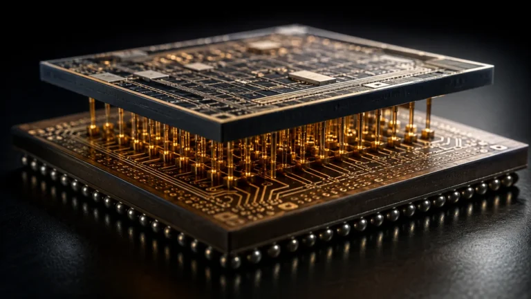
In semiconductor engineering, a standard logic gate requires two transistors to sit side-by-side (an n-type and a p-type). As we approach the 0.7-nanometer (0.7nm) era, we can no longer shrink them horizontally. Complementary FET (CFET) is the “two-story townhouse” of microchips. By stacking the two transistors vertically on top of each other, engineers drastically increase the density and computing power of an AI chip without increasing its physical size.
Why This Matters
The global semiconductor market is locked in a high-stakes arms race for the “Angstrom” era. (An Angstrom is one-tenth of a nanometer; a 1nm chip is 10 Angstroms, or A10).
TSMC, Samsung, and Intel are collectively deploying tens of billions of dollars to transition their fabrication plants to handle A14 (1.4nm) and A10 (1nm) nodes by the late 2020s. But the roadmap beyond 1nm faces a catastrophic physics barrier. The current state-of-the-art transistor—the Gate-All-Around (GAA) nanosheet—hits a performance ceiling due to the required lateral spacing between the n-type and p-type components.
To achieve the 0.7nm (A7) node slated for the early 2030s, the underlying architecture must fundamentally change. Mastering CFET is the defining hurdle that will determine which foundry dominates the next decade of artificial intelligence hardware. Failing to commercialize CFET means failing to scale computing power, effectively ending Moore’s Law.
The Big Picture
The evolution of the transistor is a battle against three-dimensional geometry.
In the 2010s, the industry moved from flat 2D transistors to FinFETs (adding a 3D vertical fin to better control electrical current). In the 2020s, the industry moved from FinFETs to GAA Nanosheets (slicing the fin into floating ribbons wrapped entirely by a gate).
As we approach 2026, research institutes like Imec are deploying a bridging technology called the Forksheet FET, which places a tiny dielectric wall between the horizontal transistors to squish them slightly closer together. However, Forksheet is only a stopgap. By completely decoupling the lateral N-to-P spacing, CFET represents the final, most complex geometric evolution of the silicon logic switch.
HOW A COMPLEMENTARY FET WORKS
Building nanoscale skyscrapers out of silicon and germanium requires atomic-level precision. Here is the first-principles breakdown.
1. The Fundamental Problem: Lateral N-P Spacing
Modern CMOS logic relies on pairs of transistors—an NFET (n-type) and a PFET (p-type). Historically, these are placed side-by-side. The physical distance between them (the N-P separation) is required to prevent electrical interference. This mandatory “empty space” puts a hard floor on how tightly you can pack transistors together, a metric measured in “track height.”
2. The Insufficiency of GAA Nanosheets
While Gate-All-Around (GAA) nanosheets successfully increased the drive current by stacking silicon ribbons vertically, they still left the NFET and PFET sitting horizontally next to each other. Even with advanced High-NA EUV lithography tools from ASML, the physical width of a side-by-side CMOS pair cannot realistically be scaled below a 5-Track (5T) cell height.
3. The Core Mechanism: Vertical Folding
CFET eliminates the lateral N-P spacing by building the NFET directly on top of the PFET (or vice versa). By sharing the exact same vertical footprint, the active area of the cell is effectively halved. This spatial liberation allows engineers to shrink the standard cell height down to a 4-Track (4T) or even 3.5T design, unlocking massive density improvements for the entire microchip.
4. Technical Depth: Monolithic vs. Sequential Integration
There are two highly contested methods for manufacturing a CFET:
- Monolithic CFET: The entire vertical stack is built simultaneously on a single silicon wafer. It involves growing a bottom channel, depositing an intermediate layer, and then growing a top channel. The challenge is “High Aspect Ratio” (HAR) etching—digging incredibly deep, microscopic trenches straight down to connect the bottom components without destroying the top ones.
- Sequential CFET: The bottom transistor is built on one wafer. A completely separate, blank silicon wafer is then molecularly bonded on top of it, and the top transistor is built on the new layer. This avoids deep-trench etching and allows the use of different, exotic channel materials. However, to avoid melting the bottom transistor, the top transistor must be manufactured at temperatures strictly below 500 degrees Celsius, which severely limits standard manufacturing processes.
5. Real-World Consequences: Backside Power Delivery
When you build a two-story transistor, routing the microscopic copper wires to both floors from the top becomes impossibly congested. To solve this, CFET strictly relies on a Backside Power Delivery Network (BSPDN). The factory flips the silicon wafer upside down and grinds away the back until the bottom of the transistor is exposed. Thick power cables are attached directly to the bottom (the “basement”), leaving the top “roof” entirely clear to route delicate data signals.
Real-World Applications
While commercial mass production of CFET is slated for the early 2030s (0.7nm era), the foundational R&D is dictating today’s hardware roadmaps.
Next-Generation AI Accelerators: An AI training superchip (like NVIDIA’s future successors to Blackwell and Vera) is entirely bound by how much Static Random-Access Memory (SRAM) and logic it can pack into the reticle limit (the maximum printable size of a chip). CFET architectures are vital for maximizing SRAM density, ensuring the chip has enough ultra-fast local memory to feed its math cores without relying constantly on slower external memory.
Mobile System-on-Chips (SoCs): Smartphone processors (such as Apple’s A-series or Qualcomm’s Snapdragon) demand extreme power efficiency in a tiny footprint. By implementing 4T CFET designs, fabless designers can drastically shrink the size of the logic blocks. This freed-up physical space on the silicon die allows manufacturers to include larger neural processing units (NPUs) or bigger batteries in the device.
Economic & Strategic Impact
The transition to CFET represents a staggering Capital Expenditure (CapEx) hurdle that threatens to thin out the top-tier foundry ecosystem.
Designing a 0.7nm fabrication plant requires ASML’s next-generation High-NA EUV lithography machines (costing roughly USD 400 million each), complex monolithic etching tools from companies like Applied Materials and Lam Research, and unprecedented precision in chemical-mechanical planarization (CMP). The cost of a single cutting-edge wafer fab at the 1nm/0.7nm node is soaring past USD 30 billion.
This is a high-stakes geopolitical gamble. Currently, only TSMC, Intel, and Samsung possess the capital, scale, and R&D pipelines necessary to participate in the Angstrom era. The extreme difficulty of aligning CFET’s multi-layer devices ensures that the technological moat protecting these three giants is virtually insurmountable for emerging competitors.
Advantages
- Ultimate Density: Crushes the standard cell track height from 5T down to 4T (and potentially 3.5T), enabling a massive leap in logic density per square millimeter.
- Wider Channels: By freeing up lateral space, engineers can actually make the transistor channels wider inside the same footprint, resulting in a stronger, faster electrical drive current.
- Reduced Routing Congestion: Paired inherently with Backside Power Delivery, the architecture physically separates signal routing from power delivery, preventing electrical interference and signal delay.
Limitations
- Severe Thermal Bottlenecks: Dissipating heat from the bottom transistor is incredibly difficult. Because it is buried beneath the top transistor, the heat struggles to escape, raising the risk of localized thermal throttling during heavy computational loads.
- Manufacturing Complexity: Monolithic integration requires atomic-level precision when etching vertical contacts. A misalignment of a single nanometer between the top and bottom source/drain contacts ruins the entire chip.
- Sequential Thermal Budgets: If the industry pivots to sequential integration, the inability to use high-heat processes (above 500 degrees Celsius) for the top wafer requires inventing entirely new laser-annealing activation techniques.
Common Misconceptions
Misconception: CFET is a form of 3D Advanced Packaging.
Reality: 3D packaging (like TSMC’s SoIC or High-Bandwidth Memory) involves stacking fully finished, separate microchips on top of each other. CFET is fundamentally different; it involves stacking the microscopic, raw atomic transistors directly on top of each other inside a single piece of silicon.
Misconception: The 0.7nm node means the transistor is physically 0.7 nanometers wide.
Reality: Node naming conventions (like 2nm, 1nm, or 0.7nm) lost their tie to physical geometric measurements over a decade ago. Today, “0.7nm” (or A7) is strictly a marketing label that signifies a specific generational leap in performance, power efficiency, and density compared to the previous generation.
Misconception: CFET will entirely replace older transistors immediately.
Reality: As with all semiconductor transitions, older architectures (like FinFET) will remain in production for decades to serve cheaper, mature technologies like IoT devices, automotive sensors, and basic microcontrollers. CFET will exclusively serve premium, high-margin AI and mobile logic.
What Most People Miss
The strategic threat of the FlipFET alternative.
While CFET is the consensus path for Western and Taiwanese roadmaps, geopolitical tech decoupling is spawning rival architectures. Recently, researchers from China’s Peking University proposed a breakthrough called “FlipFET.”
Instead of relying on the excruciatingly difficult front-side monolithic stacking required by CFET, the FlipFET process manufactures all the n-type transistors on the front of the wafer. Then, it physically flips the wafer over and manufactures all the p-type transistors on the back of the wafer. This completely avoids the deep-trench alignment problems of CFET while still achieving vertical spatial separation. While still highly experimental, breakthroughs like FlipFET highlight that the path to sub-1nm dominance is not exclusively locked behind a single Western engineering philosophy.
Comparison Table
| Feature | FinFET | GAA Nanosheet | CFET (Monolithic) |
| Primary Node Era | 14nm to 3nm | 2nm to 1.4nm (A14) | 0.7nm (A7) and beyond |
| N-P Layout | Side-by-side (Horizontal) | Side-by-side (Horizontal) | Stacked (Vertical) |
| Gate Control | 3-sided Fin wrapper | 4-sided Ribbon wrapper | Independent Top & Bottom Gates |
| Standard Cell Height | ~6T to 5T | ~5T | 4T to 3.5T |
| Power Delivery | Front-side network | Front-side or Backside | Strictly Backside Power Delivery |
| Primary Limitation | Weak current at small scale | Lateral spacing limits density | Heat dissipation & extreme complexity |
Case Study
Situation: As the semiconductor industry mapped the trajectory toward the A7 (0.7nm) node, simulation data indicated that simply shrinking existing Gate-All-Around (GAA) nanosheets would yield diminishing returns. The physical wires connecting the components would become too thin, generating massive electrical resistance that would erase any speed gains.
Challenge: The industry needed physical proof that stacking complementary devices (CFET) vertically was not just a computer simulation, but something that could actually be manufactured using existing CMOS fab equipment.
Solution (The Imec Monolithic Demonstration): At the 2024 VLSI Symposium, the Belgium-based R&D center Imec achieved a pivotal breakthrough. They successfully demonstrated, for the first time, a fully functional monolithic CMOS CFET device featuring stacked top and bottom contacts.
Outcome: Imec integrated the CFET with an 18nm gate length, a 60nm gate pitch, and a 50nm metal pitch. Crucially, they proved that by carefully sequencing epitaxial growth (growing the silicon crystals) and utilizing advanced middle-of-line contact etching, a single wafer could successfully host a functioning two-story logic gate.
Lessons Learned: This successful fabrication validated the monolithic integration pathway, giving foundries like TSMC and Intel the confidence to officially pencil CFET into their 2030+ long-term CapEx roadmaps. It proved that while the manufacturing process is incredibly complex, the fundamental physics of vertical logic stacking are completely sound.
Future Outlook
Next 12–24 Months
The industry will witness the commercial introduction of the Forksheet FET as a bridge technology. Foundries will not jump directly from standard GAA to CFET. Instead, they will insert a dielectric wall between the horizontal n-type and p-type transistors to push them closer together. Concurrently, the first commercial chips utilizing Backside Power Delivery (like Intel’s PowerVia) will hit the consumer market, serving as a critical trial run for the power routing infrastructure that CFET will eventually demand.
Next 3–5 Years
The arrival of the A10 (1nm) Pilot Lines. By 2027 and 2028, TSMC and Intel will lock in the final design rules for their 1nm processes. We will see early prototype wafers testing sequential versus monolithic CFET yields. The major equipment providers (ASML, Applied Materials) will release specialized, next-generation etching tools specifically designed to handle the High-Aspect-Ratio contact holes required to dig down into the bottom layer of the CFET stack without collapsing the structure.
Next 10 Years
The dawn of the 0.7nm (A7) Era. By the early to mid-2030s, CFET will enter mass production for flagship AI and mobile processors. The definition of a microchip will fundamentally change from a flat 2D grid into a densely populated 3D cube. Advanced iterations of CFET will likely transition away from traditional silicon channels entirely, utilizing 2D atomic materials (like Transition Metal Dichalcogenides or Tungsten Disulfide) to further reduce electrical leakage and improve speed in the absolute smallest physical footprint imaginable.
Most Likely Scenario
CFET will succeed as the undisputed architecture of the 2030s, but it will come at a severe financial cost. The astronomical expense of High-NA EUV lithography and 3D etching tools will force massive consolidation or deep joint-venture alliances among the remaining foundries. Computing power will continue to scale, but the price per transistor—which historically dropped with every new generation—will plateau, forcing AI companies to charge significant premiums for access to sub-1nm hardware.
Key Takeaways
- Complementary FET (CFET) solves the physical 2D scaling limits of microchips by vertically stacking the n-type and p-type transistors directly on top of each other.
- By eliminating the lateral empty space between transistors, CFET is expected to shrink standard cell sizes from 5T down to 4T or lower, radically improving logic density.
- The architecture is widely accepted as the mandatory successor to Gate-All-Around (GAA) nanosheets for the sub-1nm (A7 / 0.7nm) node slated for the early 2030s.
- Manufacturing CFET relies heavily on Backside Power Delivery Networks (BSPDN) to route electricity to the bottom transistor while reserving the top layer for data signals.
- The industry is fiercely debating two integration methods: Monolithic (building the stack on one wafer, facing complex etching) versus Sequential (bonding a second wafer on top, facing severe thermal limits).
- Mastering CFET will cost tens of billions in Capital Expenditure, ensuring that only apex foundries like TSMC, Intel, and Samsung will dictate the future of hardware.
Glossary
Angstrom Era: A naming convention for semiconductor nodes smaller than 1 nanometer. (1 nanometer = 10 Angstroms). The A7 node represents the 0.7nm generation.
Backside Power Delivery Network (BSPDN): An advanced chipmaking technique where the power delivery wires are moved from the top of the chip to the back of the silicon wafer, drastically reducing signal congestion on the front.
CFET (Complementary Field-Effect Transistor): A 3D transistor architecture that stacks NMOS and PMOS devices vertically.
High-NA EUV: High-Numerical Aperture Extreme Ultraviolet lithography. The newest, USD 400 million multi-story laser printers built by ASML, required to draw the microscopic patterns for 1nm and 0.7nm chips.
Monolithic Integration: A manufacturing method for CFET where the entire vertical stack of transistors is built simultaneously on a single silicon wafer.
Sequential Integration: A manufacturing method for CFET where the bottom transistor is built on one wafer, a second blank wafer is bonded on top, and the top transistor is built subsequently.
Track Height (e.g., 5T, 4T): A metric used to describe the vertical height of a standard logic cell layout. A lower number indicates a denser, more tightly packed microchip.
Frequently Asked Questions
Why can’t we just keep shrinking the current transistors?
If you make a 2D transistor any smaller, you run into quantum mechanical limits. The walls become so thin that electrons simply teleport (quantum tunnel) right through them, causing the switch to leak electricity and fail. We have to build vertically to get more performance without making the walls impossibly thin.
What is the difference between CFET and 3D Packaging?
3D Packaging (like putting a memory chip on top of a logic chip) is like stacking two finished houses on top of each other. CFET is fundamentally changing how you build the bricks inside the house. CFET stacks the raw, atomic-level transistors inside the silicon itself.
When will I be able to buy a device with a CFET chip?
Commercial mass production of CFET is not expected until the 0.7nm (A7) node, which industry roadmaps (like Imec’s) place in the 2032 to 2034 timeframe. Expect it to debut in high-end AI data center accelerators and flagship smartphones first.
How does the heat escape if a transistor is buried underneath another one?
Thermal dissipation is one of the hardest engineering challenges of CFET. The bottom transistor generates heat that is trapped by the top transistor. Engineers are developing advanced heat-conducting materials and utilizing the Backside Power Delivery copper lines acting as thermal vias to pull heat out through the bottom of the chip.
Will this make computers cheaper?
Unlikely. The historic trend of Moore’s Law making computing cheaper is slowing down. While CFET will give us vastly more powerful computers, the billions of dollars required to build these new fabrication plants means the overall cost of producing a cutting-edge chip is actually increasing.
Sources
- Tom’s Hardware: Imec Presents Sub-1nm Process and Transistor Roadmap Until 2036
- SemiWiki: CFET (Complementary FET) Industry Roadmap
- 36Kr: Wafer Foundry: Competing for 1nm Technology and the Angstrom Era
- Semiconductor Engineering: Building CFETs With Monolithic And Sequential 3D
- All About Circuits: From FinFETs to CFETs: Imec’s Plan for Continued Transistor Scaling