Advertisement
)

At a Glance
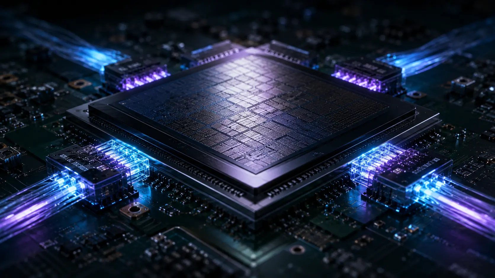
- Concept: Moving the optical transceiver (the device that converts electricity into light) from the edge of the server rack directly onto the same silicon substrate as the main processor.
- Why it matters: AI clusters require tens of thousands of GPUs to exchange terabytes of data per second. Pushing electrical signals across even a few inches of copper motherboard requires massive amounts of power and generates crippling heat. CPO solves this “I/O bottleneck.”
- Who uses it: Hyperscale cloud providers (AWS, Google, Meta), AI hardware giants (NVIDIA, Broadcom), and advanced semiconductor foundries (TSMC, GlobalFoundries).
- Biggest takeaway: CPO fundamentally changes the semiconductor supply chain. By integrating optics directly into the chip packaging, the financial value shifts away from traditional pluggable transceiver manufacturers and consolidates into the hands of the elite foundries capable of 2.5D and 3D advanced packaging.
In Simple Words
Imagine a foreign diplomat (an AI processor) who only speaks English, trying to talk to the rest of the world over a telephone line that only transmits French (fiber optic cables).
Historically, the diplomat had to shout their English message across a long, crowded room (the copper wires on a motherboard) to a translator standing by the telephone on the wall. The translator (a pluggable optical transceiver) would hear the English, translate it to French, and send it down the line.
As AI data centers got faster, the diplomat had to shout faster and louder. Shouting across the room began to require exhausting amounts of energy, generating immense heat and garbling the words.
Co-Packaged Optics (CPO) solves this by surgically implanting the translator directly into the diplomat’s vocal cords. The electrical signal no longer has to travel across the crowded motherboard. It is converted into light instantly, right where the data is processed. This saves massive amounts of electricity, drastically reduces heat, and allows the chip to communicate with the rest of the data center at the speed of light.
Why This Matters
The scaling of Artificial Intelligence is currently constrained by physics, specifically the physics of moving data.
To train frontier Large Language Models (LLMs), companies wire together clusters of 100,000 or more GPUs. These GPUs must constantly share data to synchronize their math. Moving this data accounts for up to 30% of the total power consumed by an AI data center.
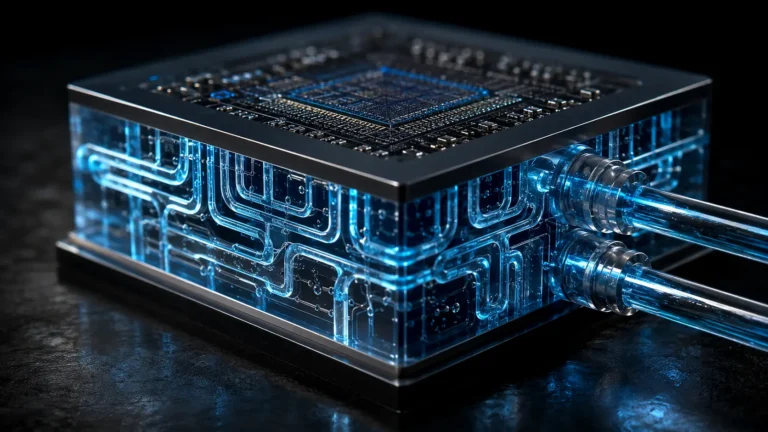
The industry measures this efficiency in picojoules per bit (pJ/bit). Driving an electrical signal across a standard copper printed circuit board (PCB) to a traditional pluggable transceiver costs roughly 15 to 20 pJ/bit. When you are moving hundreds of terabits per second, that energy cost translates into megawatts of pure heat. This heat requires massive, expensive liquid cooling infrastructure.
By integrating the optics directly next to the processor, CPO drops this energy cost down to roughly 3 to 5 pJ/bit. For hyperscalers like Microsoft and Meta, adopting CPO is not just about making networks faster; it is an existential requirement to keep their multi-billion-dollar AI data centers from exceeding the physical power limits of the local electrical grid.
The Big Picture
The transition to CPO represents the death of copper as a high-speed data medium.
For decades, the standard architecture for a data center switch was the Pluggable Form Factor (like QSFP-DD or OSFP modules). You bought a network switch, racked it, and manually plugged thumb-sized optical transceivers into the front panel.
This model worked perfectly for standard cloud computing. But the leap to 800-Gigabit (800G) and 1.6-Terabit (1.6T) networking speeds—demanded by AI workloads in 2025 and 2026—broke the pluggable model. Pushing 200 Gbps of electricity through a single microscopic copper lane (SerDes) over five inches of motherboard causes extreme signal degradation (insertion loss). To fix the degraded signal, engineers had to add power-hungry “retimer” chips, making the system even hotter and more expensive.
CPO abandons the front-panel plug. It treats photons (light) not as an external networking tool, but as an internal component of the silicon itself.
HOW CO-PACKAGED OPTICS WORKS
Shrinking a fiber-optic transmission system down to the size of a grain of rice and placing it next to a processor requires absolute mastery of photonics and materials science.
1. The Fundamental Problem: The Electrical I/O Wall
Processors (ASICs) only process electrons. Fiber optic networks only transmit photons. Every time data leaves a switch or a GPU, an electrical signal must drive a laser to pulse light on and off. The physical distance between the ASIC and the laser creates electrical resistance, capacitance, and signal loss. This is known as the Input/Output (I/O) wall.
2. The Insufficiency of Pluggable Optics
In a pluggable architecture, the laser sits on the edge of the server rack, sometimes 10 to 15 inches away from the ASIC. As signal speeds increase, high-frequency electrical signals traveling across copper behave more like radio waves, leaking out and interfering with adjacent lanes (crosstalk). Overcoming this requires blasting the signal with massive amounts of electrical power, creating unsustainable heat.
3. The Core Mechanism: Silicon Photonics and 2.5D Packaging
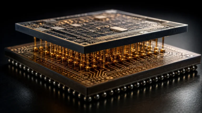
Co-Packaged Optics solves this by placing the “Optical Engine” (a microscopic silicon photonics chip) on the exact same organic substrate or silicon interposer as the main ASIC. The electrical distance drops from 10 inches to less than 10 millimeters. The ASIC sends a low-power electrical signal across this microscopic gap to a modulator on the photonic chip, which instantly encodes the data into light.
4. Technical Depth: The Thermal Paradox and External Lasers (ELS)
Here lies the greatest engineering challenge of CPO: Lasers hate heat.
A high-performance AI switch ASIC routinely operates at 90°C to 100°C. However, standard Indium Phosphide (InP) lasers begin to degrade rapidly and fail if they operate above 70°C. If you put the laser right next to the boiling hot ASIC, the laser dies.
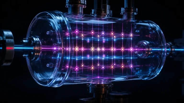
To solve this paradox, engineers developed the External Laser Source (ELS). The fragile laser is physically removed from the CPO package and plugged into the cool front panel of the server rack. It fires a “blind”, unmodulated continuous beam of light down a fiber directly into the hot CPO package. The silicon photonics chip simply acts as a shutter (a Mach-Zehnder modulator or Micro-Ring Resonator), chopping that incoming light into data without housing the heat-sensitive laser diode itself.
5. Real-World Consequences: Hyperscale Switch Densities
By removing the transceivers from the front panel and integrating them around the ASIC, network equipment manufacturers can build significantly denser switches. A single 1-Rack-Unit (1RU) switch can now handle 51.2 Terabits per second (or even 102.4T) of bandwidth, something that was physically impossible when limited by the physical faceplate area required to slot in dozens of traditional pluggable modules.
Real-World Applications
CPO is not for consumer electronics; it is strictly designed for the heaviest compute environments on Earth.
AI Backend Networks (InfiniBand & Ethernet): In an NVIDIA GPU cluster, thousands of GPUs must share data instantaneously to update the “weights” of a neural network. CPO is being heavily integrated into the spine-and-leaf network switches (like the Broadcom Tomahawk series) that route this data, ensuring that network congestion does not leave USD 40,000 GPUs sitting idle waiting for data to arrive.
Memory Disaggregation (CXL over Optics): Currently, a GPU or CPU can only access the RAM physically attached to its motherboard. If it runs out of memory, the system crashes. CPO enables “optical PCIe” and Compute Express Link (CXL) over optics. This means a processor can use light to instantly access a massive, centralized pool of memory located in a completely different server rack, with latency so low the processor thinks the memory is local.
High-Frequency Algorithmic Trading: While AI is the primary driver, quantitative hedge funds are quietly deploying CPO-enabled switches. Because CPO removes the electrical retimer chips from the signal path, it strips nanoseconds of latency out of the network hop, providing a microscopic but highly lucrative speed advantage in global arbitrage.
Economic & Strategic Impact
The shift toward CPO is violently disrupting the legacy optical networking supply chain.
For twenty years, companies like Coherent, InnoLight, and Lumentum built massive businesses assembling pluggable optical transceivers. CPO threatens to disintermediate them. Because the optics are now printed directly onto silicon and packaged alongside the processor, the economic value shifts to the semiconductor foundries (TSMC, GlobalFoundries) and the chip designers (Broadcom, NVIDIA, Marvell).
In response, legacy transceiver manufacturers are frantically pivoting to become suppliers of the External Laser Sources (ELS) or partnering with foundries to offer specialized silicon photonics design services.
Strategically, CPO enforces the dominance of TSMC. Advanced packaging technologies like TSMC’s COUPE (Compact Universal Photonic Engine) are required to stack these optical and electrical chips together with microscopic precision. The nations and companies that control the advanced packaging supply chain will ultimately control the velocity of global AI infrastructure.
Advantages
- Massive Power Reduction: Decreases optical interconnect power consumption by up to 50%, saving megawatts of power across a hyperscale data center.
- Bandwidth Density: Unlocks 51.2T and 102.4T switch capacities by bypassing the physical space limits of front-panel pluggable ports.
- Reduced Latency: Eliminates the need for power-hungry electrical DSP (Digital Signal Processing) and retimer chips on the motherboard, streamlining the data path.
- Cost at Scale: While initial R&D is astronomical, printing optical engines on 300mm silicon wafers via standard CMOS foundry processes will eventually drive the per-gigabit cost of optics below that of hand-assembled pluggables.
Limitations
- The “Blast Radius” Yield Problem: If a traditional pluggable transceiver breaks, a technician unplugs it and slots in a $1,000 replacement. If one microscopic optical lane dies inside a CPO package, the entire $50,000 ASIC switch is ruined. This extreme sensitivity to manufacturing yields has been the primary barrier to mass adoption.
- Serviceability: You cannot hot-swap a co-packaged optic. It requires tearing down the server and replacing the entire compute board.
- Ecosystem Standardization: Pluggable optics work because they adhere to strict Multi-Source Agreements (MSAs)—any brand fits in any slot. CPO currently lacks strict standardization; a Broadcom CPO engine does not interface identically to a Marvell or NVIDIA design, creating dangerous vendor lock-in for cloud providers.
Common Misconceptions
Misconception: CPO means the computer chip actually processes light instead of electricity.
Reality: The main processor (CPU/GPU/Switch ASIC) still strictly processes electrons. CPO just moves the converter (the silicon photonics engine) onto the same physical package. True “optical computing” (using light to do the actual math) is an entirely different, highly experimental field.
Misconception: Pluggable transceivers will disappear immediately.
Reality: Pluggables will coexist with CPO for at least another decade. CPO is only economically viable at the extreme edge of networking (1.6T and beyond). For standard enterprise data centers running 100G or 400G networks, pluggables remain vastly cheaper, highly reliable, and easily serviceable.
Misconception: CPO places a microscopic laser onto the silicon chip.
Reality: While some early designs attempted this, the industry largely pivoted to External Laser Sources (ELS). Lasers are too fragile to survive the intense heat generated by an AI processor, so the actual laser remains plugged into the front of the server rack, safely away from the heat.
What Most People Miss
The hidden enabler of CPO is Advanced Semiconductor Packaging, not just photonics.
Printing a silicon photonics chip is relatively easy in 2026. The true engineering miracle is attaching a glass fiber-optic cable to a silicon chip with sub-micron precision, and then connecting that photonic chip to a massive logic ASIC using tens of thousands of microscopic copper bumps (microbumps or TSVs). This requires cleanrooms, thermal compression bonding, and interposer technologies. The narrative around CPO often focuses on light, but the actual battleground is the mechanical engineering of aligning microscopic glass to hot silicon without it cracking.
Comparison Table
| Feature | Copper Cables (DAC) | Pluggable Optics (e.g., OSFP/QSFP) | Co-Packaged Optics (CPO) |
| Data Medium | Electrons | Electrons to Photons (at rack edge) | Electrons to Photons (on chip package) |
| Max Practical Speed | Low (Limits hit at high speeds) | High (Up to 800G/1.6T) | Extreme (1.6T to 6.4T per engine) |
| Power Efficiency | High (for very short distances) | Low (~15-20 pJ/bit) | Excellent (~3-5 pJ/bit) |
| Serviceability | Easy (Hot-swappable) | Easy (Hot-swappable) | Extremely Difficult (Fused to ASIC) |
| Signal Distance on Motherboard | Inches to Meters | 5 to 15 Inches | < 10 Millimeters |
Case Study
Situation: As hyperscale cloud providers laid out their roadmaps for next-generation generative AI clusters in 2024 and 2025, network switch manufacturers realized that scaling traditional pluggable architectures to 51.2 Terabits per second (51.2T) was pushing the physical limits of power and cooling.
Challenge: Broadcom, the dominant supplier of hyperscale networking chips, needed to deliver a 51.2T switch (the Tomahawk 5 series) that didn’t consume an unsustainable portion of the data center’s power budget or require impossibly large heat sinks.
Solution (The Integration): Broadcom successfully launched the “Bailly” 51.2T CPO switch. Instead of relying on 64 separate 800G pluggable transceivers on the front panel, Broadcom packaged eight 6.4T silicon photonics engines directly around the Tomahawk 5 ASIC on a single substrate. They utilized External Laser Sources (ELS) housed on the front panel to feed light to the package, bypassing the thermal paradox.
Outcome: The Bailly CPO switch reduced optical power consumption by a staggering 70% compared to equivalent pluggable solutions. By removing the electrical retimer chips from the motherboard, it also reduced the overall system cost and latency.
Lessons Learned: The deployment proved that CPO is no longer an R&D science project. It validated that heterogeneous packaging—combining a monolithic silicon ASIC with separate silicon photonics chiplets—is the only mathematically and thermally viable path forward for hyperscale AI networking.
Future Outlook
Next 12–24 Months
The industry will move through the “hybrid” phase. Cloud providers will deploy Linear Drive Pluggable Optics (LPO)—a stopgap technology that removes the power-hungry DSP chips from pluggable modules without forcing a full redesign to CPO. However, as 1.6T per-port speeds become the baseline for top-tier AI training clusters, the power limits of LPO will be exposed, forcing the heaviest AI operators (Microsoft, Meta, AWS) to commit fully to early CPO architectures.
Next 3–5 Years
We will see the rise of Optical I/O for GPUs, not just network switches. Currently, CPO is primarily used in the network switches that connect servers together. The next leap is putting CPO directly onto the NVIDIA or AMD GPU package itself. This will allow GPUs to communicate directly with each other via light, completely bypassing traditional network interface cards (NICs) and unleashing an era of exponentially faster, optically-bound supercomputers.
Next 10 Years
Standardization will conquer the “blast radius” yield problem. Just as the semiconductor industry developed the UCIe (Universal Chiplet Interconnect Express) standard for silicon chiplets, the optical industry will establish universal standards for attaching photonic engines to organic substrates. Wafer-scale optical integration will become a standard foundry process, dropping the cost of CPO to levels where it begins penetrating mid-tier enterprise data centers, definitively ending the reign of copper in server architecture.
Most Likely Scenario
CPO will not eradicate pluggable optics immediately, but it will absolutely dominate the top 10% of the market where AI hyperscaling occurs. The sheer physics of moving trillions of parameters per second dictates that data must be converted to light as close to the silicon as physically possible. The companies that command the 2.5D and 3D packaging technologies required to fuse glass to silicon will become the undisputed gatekeepers of the 21st-century compute infrastructure.
Key Takeaways
- Co-Packaged Optics (CPO) integrates silicon photonics directly onto the processor’s packaging, minimizing the distance electrical signals must travel before being converted to light.
- Driving high-speed electrical signals across copper motherboards to traditional pluggable transceivers generates massive heat and requires unsustainable amounts of power.
- By solving the “I/O bottleneck,” CPO drops optical power consumption from ~15 pJ/bit down to ~5 pJ/bit, a critical requirement for scaling AI data centers.
- Because lasers degrade in high heat, most CPO designs use an External Laser Source (ELS) plugged into the front panel, feeding “blind” light via fiber into the hot CPO package to be modulated.
- CPO shifts the economic value of optical networking away from traditional transceiver assemblers and toward advanced semiconductor foundries (like TSMC) and chip designers (like Broadcom).
- The primary barriers to CPO adoption are poor serviceability (it is not hot-swappable) and strict manufacturing yields (one broken optical lane ruins the entire expensive processor).
Glossary
Co-Packaged Optics (CPO): The advanced packaging technology that places a silicon photonics engine on the same substrate as a digital processor (ASIC) to reduce electrical signal distance.
External Laser Source (ELS): A laser module plugged into the front of a server rack, separate from the CPO package. It feeds continuous, unmodulated light via fiber to the silicon photonics chip, protecting the fragile laser from the processor’s extreme heat.
Insertion Loss: The loss of signal power that occurs when an electrical signal travels through a medium (like copper traces on a motherboard). High speeds cause higher insertion loss.
Pluggable Optics: The traditional network architecture where optical transceivers are housed in metal cartridges and manually plugged into ports on the front panel of a network switch.
SerDes (Serializer/Deserializer): The microscopic electrical lanes on a chip that convert data into a high-speed serial stream to be sent out of the processor. Pushing SerDes speeds to 100G or 200G over copper is the root cause of the power wall.
Silicon Photonics: The practice of building optical components (like modulators and waveguides) using the exact same silicon manufacturing techniques used to build standard computer chips, allowing for mass production of microscopic optical engines.
Frequently Asked Questions
Why does moving the optic closer to the chip save power?
Electrical resistance. Pushing a high-frequency electrical signal through 10 inches of copper motherboard requires powerful amplifiers to ensure the signal doesn’t degrade before it reaches the transceiver. If the distance is 10 millimeters instead of 10 inches, you don’t need those heavy amplifiers, saving massive amounts of electricity.
If one part of a CPO switch breaks, do you have to replace the whole thing?
Currently, yes. This is the biggest drawback. Unlike pluggable optics, where you can simply pull out a broken $1,000 module and slide in a new one, a failed optical engine in a CPO system usually means the entire expensive switch must be pulled from the rack and sent back to the manufacturer.
Is CPO being used right now?
Yes, but in limited, high-end hyperscale deployments. In 2025 and 2026, tech giants like Meta and Google began deploying top-of-rack CPO switches (like Broadcom’s 51.2T Bailly) specifically to manage the extreme bandwidth demands of their newest AI training clusters.
Does an NPU (Neural Processing Unit) use CPO?
Eventually, yes. Currently, NPUs in laptops or edge devices do not need CPO because they are not moving terabytes of data across a data center. However, massive AI accelerators (GPUs/NPUs) in cloud servers are the primary target for future CPO integration.
What is Linear Drive Pluggable Optics (LPO)?
LPO is a competitor/stepping-stone to CPO. It keeps the familiar pluggable format but removes the power-hungry internal processing chips (DSP) from the module, relying on the main processor to drive the signal. It saves power but does not fully solve the physical density problem that CPO solves.
Sources
- Broadcom Inc.: Tomahawk 5 and Bailly 51.2T Co-Packaged Optics Architecture (2025)
- Yole Intelligence: Silicon Photonics and Co-Packaged Optics Market Forecast 2026-2033
- TSMC Technology Symposium: COUPE (Compact Universal Photonic Engine) and Advanced 3D Packaging
- Optical Internetworking Forum (OIF): External Laser Small Form Factor Pluggable (ELSFP) Implementation Agreements