Advertisement
)

At a Glance
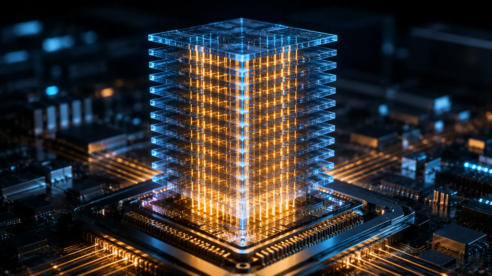
- Concept: A revolutionary memory architecture that stacks 12 to 16 layers of DRAM vertically on top of a customized logic processor, connected by thousands of microscopic internal electrical pillars.
- Why it matters: Frontier AI models contain trillions of parameters. Without HBM4, processors like NVIDIA’s Blackwell and AMD’s Instinct accelerators would sit idle, burning power while waiting for data to travel across a traditional motherboard.
- Who uses it: AI hyperscalers, advanced autonomous driving systems, and elite semiconductor designers leveraging the manufacturing duopoly of SK Hynix (partnered with TSMC) and Samsung Electronics.
- Biggest takeaway: HBM4 changes the definition of memory. The bottom layer of the HBM4 stack is now an advanced logic die (printed on 3nm or 4nm nodes). This turns the memory module into a localized “co-processor” capable of repairing itself, routing its own data, and reducing the computational burden on the main GPU.
In Simple Words
Imagine a massive, ultra-fast factory (an AI processor) that builds cars.
Historically, the warehouse holding all the car parts (traditional RAM) was located in a different city. To get parts to the factory, you had to load them onto trucks and drive them down a single-lane highway (a traditional memory bus). No matter how fast the factory worked, it was constantly forced to stop and wait for the trucks to arrive.
High Bandwidth Memory (HBM) solved this by moving the warehouse directly next door to the factory and building a 1,024-lane superhighway between them.
HBM4 is the 2026 upgrade. It stacks 16 warehouses directly on top of each other, right next to the factory. To move the parts, it doubles the superhighway to 2,048 lanes. Furthermore, the basement of this new warehouse is run by an advanced computer manager (the logic base die) who organizes the parts before they even hit the highway. The factory never stops, allowing the AI to process massive amounts of data at the speed of light.
Why This Matters
The semiconductor industry is fighting a brutal war against physics known as the “Memory Wall.”
In 2026, compute power is cheap, but moving data is astronomically expensive. If a hyperscale AI data center attempts to train a multi-trillion-parameter large language model using older memory technology, the GPUs spend over 60% of their time idle, waiting for data. In a billion-dollar data center, idle GPUs are an unacceptable destruction of capital.
HBM4 is the only physical solution to this bottleneck. By pushing memory bandwidth over 3.0 Terabytes per second (TB/s) per stack and expanding capacity up to 64 Gigabytes (GB) per stack, a single flagship GPU utilizing eight HBM4 modules can hold over 500GB of memory. This allows AI models to remain entirely inside the GPU’s localized memory rather than being painfully partitioned across hundreds of different servers. Consequently, whoever controls the HBM4 supply chain dictates the deployment speed of the global artificial intelligence economy.
The Big Picture
The leap from HBM3e (the 2024/2025 standard) to HBM4 is not an incremental speed upgrade—it is a fundamental tear-down and redesign of semiconductor architecture.
In early 2025, JEDEC (the global semiconductor standardization body) published the JESD270-4 specification for HBM4. The critical mandate was a transition from a 1,024-bit interface to a 2,048-bit interface.
While doubling the interface sounds simple, it triggered an engineering nightmare for printed circuit board (PCB) and silicon interposer designers. You cannot simply drop an HBM4 module into an older HBM3e slot; the pin density is too high. This explosion in routing complexity forces the industry to rely heavily on advanced 2.5D and 3D packaging technologies (like TSMC’s CoWoS—Chip on Wafer on Substrate) to physically connect the memory to the processor without the microscopic wires crossing and short-circuiting.
HOW HBM4 WORKS
Building a 16-story skyscraper of memory requires manipulating silicon at an atomic scale. Here is the first-principles breakdown of HBM4.
1. The Fundamental Problem: Distance and Power
Moving an electron across a two-inch copper trace on a motherboard requires a massive amount of electrical voltage to overcome resistance. This burns immense power and generates heat. To make memory faster, you must place the memory chips as physically close to the processor as possible.
2. The Insufficiency of Traditional GDDR
Graphics Double Data Rate (GDDR) memory places chips flat on a circuit board around the processor. Because it is flat (2D), you quickly run out of physical real estate around the GPU. To get more memory, you have to place chips further away, which re-introduces the latency and power problem.
3. The Core Mechanism: Through-Silicon Vias (TSVs)
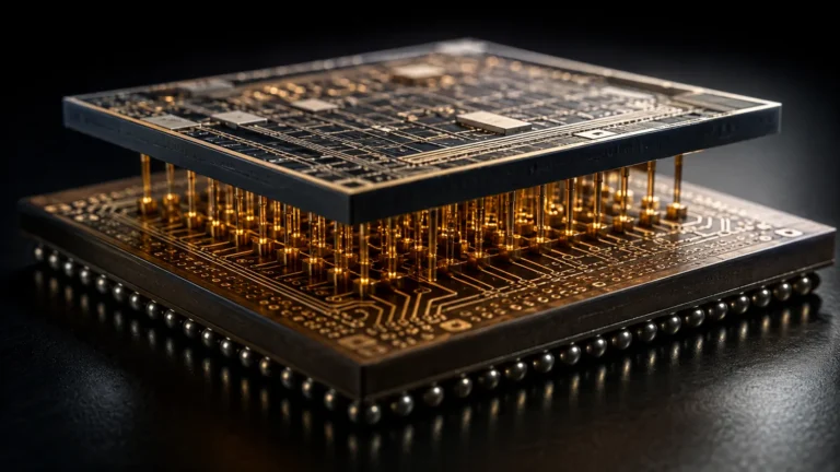
HBM4 solves the space problem by building upward. Engineers take ultra-thin DRAM memory dies and stack them vertically (up to 16 layers high). To connect these layers, they use Through-Silicon Vias (TSVs). A laser drills thousands of microscopic holes directly through the center of the silicon memory chips. These holes are filled with copper, creating vertical elevator shafts that allow data to travel straight down the stack into the processor, rather than traveling outward across a circuit board.
4. Technical Depth: Advanced Packaging (MR-MUF vs. Hybrid Bonding)
Connecting these incredibly thin layers without them cracking is the ultimate manufacturing bottleneck.
- Advanced MR-MUF (Mass Reflow Molded Underfill): Pioneered by SK Hynix, this process involves stacking the chips with tiny micro-bumps of solder between them, melting the solder in an oven, and then injecting a liquid epoxy resin into the microscopic gaps to glue the skyscraper together and conduct heat outward.
- Hybrid Bonding: The theoretical endgame. It completely removes the solder bumps and the underfill. Instead, the flat copper pads of one chip are perfectly aligned with the flat copper pads of another and fused together at the atomic level using heat and pressure.
Intelligence Note: While Hybrid Bonding was heavily anticipated for HBM4, JEDEC recently relaxed the total thickness constraints for HBM4 to 900+ micrometers in July 2026. This leniency allowed manufacturers to delay the highly expensive Hybrid Bonding transition until the subsequent HBM4E/HBM5 generations, opting to squeeze the final life out of their refined micro-bump (MR-MUF and TC-NCF) techniques.
5. Real-World Consequences: The Thermal Wall
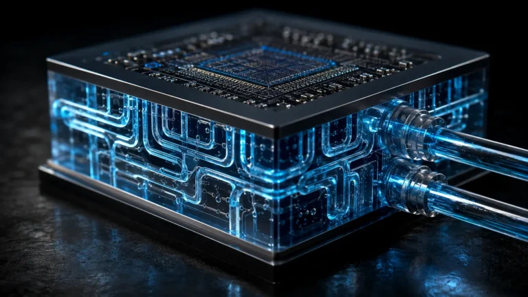
The downside of a 16-layer stack is thermodynamics. When you stack 16 layers of silicon on top of a highly active logic base die, the heat generated in the middle of the stack has nowhere to go. The silicon layers act like thermal blankets, insulating the heat. HBM4 requires unprecedented liquid cooling architectures to prevent the memory stack from literally cooking itself from the inside out.
Real-World Applications
HBM4 is exclusively deployed in high-performance computing (HPC) environments where bandwidth outweighs cost.
Next-Generation AI Accelerators: The NVIDIA “Rubin” and “Feynman” platform architectures, alongside AMD’s Instinct MI400/MI500 series, are the primary consumers of HBM4. By utilizing HBM4’s 2,048-bit bus, these GPUs can access data at over 3.3 TB/s per stack. With an 8-stack configuration, a single GPU can chew through 26 TB/s of bandwidth, allowing real-time, low-latency inference for multimodal AI models (processing text, video, and audio simultaneously).
Custom Supercomputing (ASICs): Hyperscale cloud providers like Google (TPU), Amazon (Trainium), and Meta (MTIA) design their own custom AI silicon. HBM4 introduces the “Custom Logic Base Die.” This allows Google, for example, to ask TSMC to embed specific tensor-routing algorithms directly into the bottom layer of their purchased HBM4 stacks, creating a highly proprietary memory module perfectly optimized for Google’s internal software.
Autonomous Driving and Edge AI: While currently too expensive for consumer vehicles, advanced Level 5 autonomous driving research units use localized HBM-equipped processors in the trunk of the vehicle to process dozens of 4K LIDAR and camera streams in milliseconds, where a split-second delay in memory retrieval could result in a fatal crash.
Economic & Strategic Impact
The transition to HBM4 has triggered an unprecedented realignment of the global semiconductor supply chain.
Historically, memory was a pure commodity. Companies like Samsung, SK Hynix, and Micron built generic DRAM chips and sold them in bulk.
HBM4 shatters this model because of the Logic Base Die. The bottom layer of an HBM4 stack requires advanced logic manufacturing (like a 3nm or 4nm process). Pure memory companies do not have state-of-the-art logic foundries.
This forces deep, strategic partnerships. SK Hynix (the dominant market leader in HBM3e) cemented its dominance by partnering directly with TSMC. SK Hynix provides the memory layers; TSMC prints the 3nm logic base die and handles the final CoWoS packaging. Conversely, Samsung Electronics holds a unique, vertically integrated advantage: they own a memory division, an advanced logic foundry (4nm), and a packaging division, allowing them to build custom HBM4 entirely in-house.
For investors, HBM is no longer a memory play; it is a custom packaging and foundry integration play.
Advantages
- Extreme Bandwidth at Lower Power: By doubling the bus width to 2,048 bits, HBM4 achieves higher throughput without cranking up the clock speeds, allowing a 60% power efficiency improvement and dropping the core voltage to 1.05V (down from 1.1V in HBM3e).
- Massive VRAM Capacity: Scaling to 16-High stacks with 32-gigabit (Gb) density allows up to 64GB of memory per module. An 8-stack server can hold 512GB of unified memory, solving the parameter-capacity crisis.
- Customization: The logic base die allows AI hardware designers to integrate security, compression, and error-correction directly into the memory hardware, offloading work from the main GPU.
Limitations
- Astronomical Cost: HBM4 is an intricately packaged, multi-die system that relies on extreme “Known Good Die” (KGD) yields. If one memory layer in a 16-High stack is defective, the entire expensive stack is ruined and thrown away.
- The Interposer Bottleneck: Connecting a 2,048-bit wide memory module to a GPU requires a silicon interposer with microscopic routing. This stretches the limits of packaging physics, creating massive production bottlenecks at foundries like TSMC.
- No Backward Compatibility: Because the physical pin layout and the fundamental architecture changed drastically to accommodate the wider bus, hardware companies cannot simply upgrade an older HBM3e server with HBM4. It requires entirely new silicon designs from the ground up.
Common Misconceptions
Misconception: HBM4 memory is physically “faster” than regular DDR5 memory.
Reality: The actual memory cells inside HBM4 operate at relatively normal speeds. HBM achieves its massive bandwidth not by being insanely fast, but by being incredibly wide. DDR5 uses a 64-bit channel. HBM4 uses a 2,048-bit channel. It is a massive, multi-lane highway moving traffic at a steady speed, rather than a single-lane road with racecars.
Misconception: Hybrid Bonding is required to make HBM4 work.
Reality: As of late 2026, manufacturers discovered they could squeeze 16-layer stacks into JEDEC’s relaxed 900-1000 micrometer thickness guidelines using advanced micro-bump technologies (like MR-MUF). The hyper-expensive, true copper-to-copper Hybrid Bonding is being largely delayed for HBM4E and HBM5.
Misconception: HBM will replace the RAM in your laptop.
Reality: HBM is fused directly to the processor package and cannot be upgraded by the user. It is highly inflexible, runs extremely hot, and is vastly too expensive for consumer devices. Traditional LPDDR and CAMM2 memory will continue to dominate laptops and phones.
What Most People Miss
The true engineering triumph of HBM4 is Directed Refresh Management (DRFM).
Standard DRAM must constantly “refresh” its electrical charge, or it forgets its data. In an ultra-hot, 16-story skyscraper of memory, heat causes electrons to leak faster, meaning the memory must refresh more often, which burns even more power and causes the GPU to wait. DRFM is a new, highly advanced reliability feature built into the HBM4 logic base die that actively targets and manages specific, high-risk memory rows without locking down the entire memory bank, preventing the thermal physics of 3D stacking from destroying data integrity.
Comparison Table
| Feature | HBM3e (The 2024/2025 Standard) | HBM4 (The 2026 Shift) | HBM4E (The 2027 Evolution) |
| Bus Width (Interface) | 1,024-bit | 2,048-bit | 2,048-bit |
| Peak Bandwidth per Stack | ~1.2 TB/s | 2.0 TB/s to 3.3 TB/s | Up to 4.0 TB/s |
| Max Capacity per Stack | 36 GB (12-High) | 64 GB (16-High) | 64 GB+ (16-High) |
| Base Die Process | Standard Memory Interface | Advanced Logic Node (TSMC 3nm / Samsung 4nm) | Advanced Logic Node |
| Core Voltage | 1.1V | 1.05V | Optimized |
| Packaging Architecture | Micro-bumps | Advanced Micro-bumps (MR-MUF / TC-NCF) | Impending transition to Hybrid Bonding |
Case Study
Situation: As AI scaling laws dictated the creation of multi-trillion parameter models, NVIDIA and AMD realized that their next-generation accelerators would be fundamentally bottlenecked by the 1,024-bit interface of HBM3e. They needed a massive jump in bandwidth, but pushing voltages higher would breach the thermal limits of the data center.
Challenge: Expanding the bus to 2,048 bits for HBM4 required an entirely new logic base die and pushed the limits of how tall a memory stack could physically be before the microscopic solder bumps cracked under thermal stress.
Solution (The Hynix/TSMC Alliance): Recognizing that a standard memory company could not fabricate an advanced logic base die, SK Hynix formed a strategic, high-profile alliance with TSMC. SK Hynix utilized its proprietary 1b DRAM process and its proven Advanced MR-MUF packaging to stack the memory, while outsourcing the highly complex logic base die directly to TSMC to be printed on a 3nm/12nm node.
Outcome: By September 2025/early 2026, SK Hynix successfully transitioned its HBM4 into mass production. By retaining MR-MUF and leveraging TSMC’s logic superiority, they hit the 2,048-bit requirement and maintained their position as the preferred supplier for NVIDIA’s most advanced platforms. Simultaneously, Samsung aggressively launched its own HBM4 using a fully in-house 4nm logic substrate, creating a fierce duopoly.
Lessons Learned: The era of isolated semiconductor manufacturing is over. Achieving the thermal and bandwidth requirements of HBM4 proved that “Memory-Logic Integration” is the only viable path forward. Success in the AI supercycle requires either absolute in-house vertical integration (Samsung) or flawless, cross-border foundry partnerships (SK Hynix/TSMC).
Future Outlook
Next 12–24 Months
The second half of 2026 and throughout 2027 will be defined by the fierce rollout of HBM4E. While HBM4 establishes the 2,048-bit baseline, HBM4E acts as the aggressive overclock, pushing pin speeds from 8 Gbps to 16 Gbps and driving single-stack bandwidth to an astonishing 4.0 TB/s. The major bottleneck during this period will be TSMC’s CoWoS packaging capacity, as cloud hyperscalers furiously outbid each other for access to the finite supply of completed memory-GPU packages.
Next 3–5 Years
The physical limits of solder will force the adoption of Hybrid Bonding. As the industry looks toward HBM5 (around 2028-2029), JEDEC thickness relaxations will no longer save manufacturers. The need to stack 20 or 24 layers of memory within a millimeter of space will make micro-bumps obsolete. The industry will transition entirely to fluxless, copper-to-copper direct hybrid bonding, marking one of the most expensive capital expenditure cycles in the history of semiconductor equipment manufacturing.
Next 10 Years
HBM will begin to merge seamlessly into the processor architecture itself via 3D Logic-on-Memory integration. Rather than placing a GPU next to an HBM stack on a 2.5D interposer, true 3D ICs will stack the processing cores directly on top of the memory arrays. This ultimate convergence will effectively erase the distinction between where data is stored and where math is calculated, paving the way for Artificial General Intelligence (AGI) hardware that mimics the localized, high-efficiency structure of the human brain.
Most Likely Scenario
HBM4 guarantees that the rapid pace of AI model scaling will not crash into a hardware wall before the end of the decade. However, the extreme cost and complexity of integrating a 2,048-bit, logic-based memory stack ensure that the global AI infrastructure market will remain highly monopolized. Only a handful of elite foundries and hyper-capitalized tech giants will possess the financial and engineering resources to participate in the HBM4 ecosystem.
Key Takeaways
- HBM4 is the 2026 standard for AI memory, doubling the physical interface to 2,048 bits to deliver over 3.0 TB/s of bandwidth per stack.
- Instead of standard memory interfaces, HBM4 integrates an advanced, custom logic base die (built on 3nm or 4nm nodes), effectively turning the memory stack into an intelligent co-processor.
- The chips are stacked up to 16 layers high and connected internally using Thousands of Through-Silicon Vias (TSVs), eliminating the power waste of routing signals across a traditional motherboard.
- Because of relaxed JEDEC thickness guidelines, manufacturers like SK Hynix are delaying highly expensive Hybrid Bonding, relying instead on advanced micro-bump technologies (MR-MUF) for initial HBM4 production.
- The necessity of advanced logic base dies has permanently altered the supply chain, forcing deep integration between memory specialists (SK Hynix) and elite logic foundries (TSMC).
- Without HBM4, the next generation of multi-trillion parameter AI models from NVIDIA, AMD, and hyperscalers would be physically incapable of processing data efficiently.
Glossary
Advanced Packaging (2.5D / 3D): Techniques used to combine multiple separate silicon chips (like GPUs and HBM) into a single, tightly integrated package using a silicon interposer, drastically increasing data transfer speeds.
Base Die: The foundational bottom layer of an HBM stack. In HBM4, this layer has evolved from a simple data router into an advanced logic processor capable of running custom diagnostic and power management algorithms.
Hybrid Bonding: An ultra-advanced packaging technique that fuses chips together directly using flat copper pads without any solder or bumps, allowing for extreme miniaturization.
MR-MUF (Mass Reflow Molded Underfill): A proprietary SK Hynix packaging process that injects liquid protective material into the gaps between stacked chips, offering high efficiency and strong thermal dissipation.
The Memory Wall: The growing disparity between how fast a CPU/GPU can process data and how slowly the RAM can deliver that data, resulting in wasted, idle compute time.
Through-Silicon Via (TSV): A microscopic, vertical electrical connection (via) that passes completely through a silicon wafer or die, allowing stacked chips to communicate directly up and down.
Frequently Asked Questions
Why is HBM4 necessary if HBM3e is already fast?
HBM3e maxed out the efficiency of a 1,024-bit bus. To get more bandwidth, engineers had to crank up the clock speeds, which generated too much heat and used too much power. HBM4 doubled the bus to 2,048 bits, allowing the system to move twice the data at a lower, more stable voltage.
Does my gaming PC use HBM4?
No. HBM4 is strictly designed for enterprise data centers and hyperscale AI accelerators. It is far too expensive, difficult to cool, and complex to manufacture for consumer-grade graphics cards, which will continue to rely on GDDR7 memory.
Why did JEDEC change the thickness rules for HBM4?
Squeezing 16 layers of DRAM and a base die into 775 micrometers (the old limit) was proving impossibly difficult without adopting brand new, expensive Hybrid Bonding machines. By relaxing the limit to 900+ micrometers, JEDEC allowed manufacturers to maintain their current, proven packaging techniques (like MR-MUF) for one more generation to meet the massive, immediate AI demand.
What is the difference between SK Hynix’s and Samsung’s approach?
SK Hynix is a pure memory player, so they partnered with TSMC to manufacture the complex logic base die. Samsung Electronics has both a memory division and an advanced logic foundry, allowing them to manufacture the entire 4nm logic base die and the 1c DRAM stack completely in-house.
Why is heat such a big problem for HBM4?
When you stack 16 layers of silicon, the heat generated by the logic die at the bottom and the data flowing through the TSVs gets trapped in the middle layers. Silicon acts as an insulator. Managing this “thermal wall” to prevent the memory cells from degrading is the primary reason advanced liquid cooling is becoming mandatory in AI data centers.
Sources
- Siemens Digital Industries Software: HBM3e and HBM4 IC design guide for next-generation high bandwidth memory (April 2026)
- Ersa Electronics: HBM4 compared to HBM4E – Mass Production Timelines and JEDEC Standards (June 2026)
- Wccftech / ZDNet: Hybrid Bonding and Relaxed JEDEC Rules for HBM4 Thickness (July 2026)
- SK Hynix Newsroom: Vision at TSMC Symposium – Integration of Memory and Logic (April 2026)
- Samsung Electronics Global Newsroom: Samsung Unveils HBM4E and Comprehensive AI Solutions at NVIDIA GTC 2026 (March 2026)
- Econ Market Research: Top High-Bandwidth Memory Companies to Watch in 2026