Advertisement
)

AT A GLANCE
- Concept: Through-Silicon Via (TSV): Microscopic vertical copper tunnels drilled directly through silicon chips to pass electrical signals.
- Concept: Silicon Interposer: A highly engineered foundation plate that routes data between the processor and the memory stack.
- Concept: Microbumps: Tiny solder connections that glue the stacked memory chips together and conduct data.
- Concept: The Memory Wall: The physical limitation where processors calculate data much faster than memory can deliver it.
IN SIMPLE WORDS
Imagine a world-class chef working in a professional kitchen. The chef can chop vegetables incredibly fast.
However, if the chef’s ingredients are stored in a warehouse across town, their cutting speed does not matter. The chef will spend most of the day standing around waiting for the delivery truck. This is the exact problem facing modern artificial intelligence. The graphics processing units (GPUs) are incredibly fast, but standard computer memory sits too far away on the motherboard, causing massive delays.
High-Bandwidth Memory solves this by moving the warehouse directly onto the chef’s cutting board. Instead of placing memory chips flat on the motherboard, engineers stack them vertically like a high-rise building. They drill microscopic tunnels straight down through the floors of the building, allowing massive amounts of data to drop directly into the processor instantly. This prevents the processor from ever waiting for data.
HOW IT WORKS
To understand HBM, you must first understand the bottleneck of traditional memory like DDR5. Standard memory chips sit on the motherboard and communicate with the processor across a narrow physical wire bus. This creates severe physical latency.
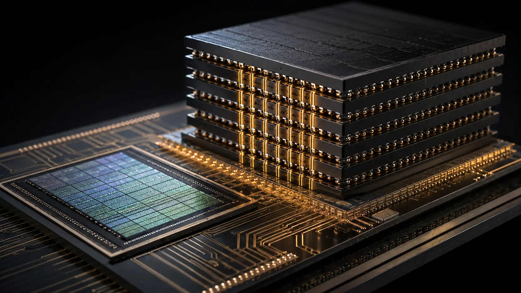
HBM radically alters this physical geography using 2.5D advanced packaging. The processor and the memory chips are removed from the main motherboard and placed side-by-side onto a silicon interposer. This interposer is a microscopic, ultra-dense routing layer embedded with tens of thousands of copper wires.
Instead of spreading memory chips out horizontally, HBM stacks them vertically. A modern HBM3e stack consists of 8 or 12 individual Dynamic Random Access Memory (DRAM) dies layered on top of a foundational logic base die.
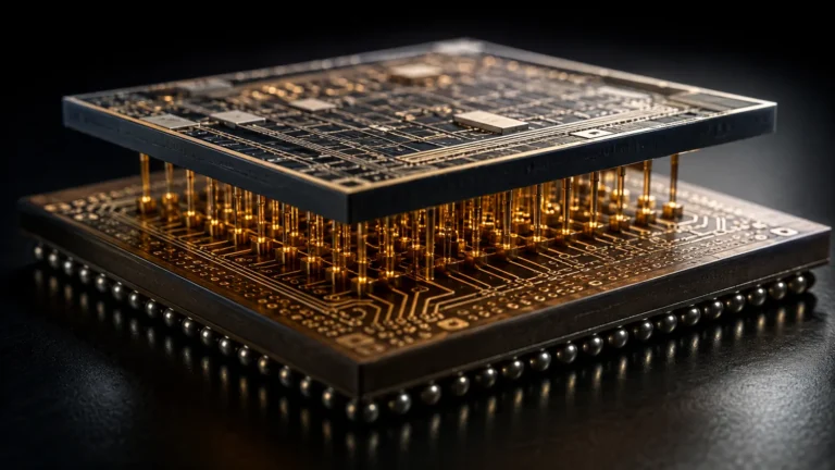
Connecting these vertical layers requires Through-Silicon Vias (TSVs). Engineers drill thousands of microscopic holes directly through the crystalline silicon of each memory die and fill them with copper.
Between each die layer, microscopic solder spheres known as microbumps fuse the TSVs together. This creates thousands of vertical data highways. Because the memory is so physically close to the processor and connected by such a massive number of lanes, the data bus width expands from a standard 64 bits to an astounding 1024 bits per stack.
This extreme physical proximity and wide data path allow HBM to deliver terabytes of data per second while consuming significantly less electricity than traditional memory architectures.
REAL WORLD EXAMPLE
The Nvidia H100 Tensor Core GPU, the engine powering the current artificial intelligence boom, relies entirely on HBM. The actual computing brain of the H100 is surrounded by six stacks of HBM3 memory provided largely by South Korean manufacturer SK Hynix.
If Nvidia attempted to feed the H100 processor using standard DDR memory, they would need a motherboard larger than a dining room table to fit the necessary wiring, and the electrical resistance of those long wires would melt the components. By using HBM3, Nvidia achieves an aggregate memory bandwidth of over 3 terabytes per second within a chip package no larger than a coaster.
WHY IT MATTERS NOW
Artificial intelligence fundamentally operates on a bottleneck of data movement, not math calculation. Large Language Models (LLMs) contain hundreds of billions of parameters. To generate a single word, the system must read nearly every single parameter stored in the memory.
If the memory cannot move these parameters into the computing core fast enough, the expensive processor sits idle. This is known as the “Memory Wall.” High-Bandwidth Memory is currently the only commercial technology capable of breaking this wall, making it the absolute limiting factor for the entire AI industry.
Because of this, HBM has created the most severe supply chain chokepoint in modern electronics. Producing HBM is notoriously difficult. Drilling TSVs through microscopic silicon without shattering the die results in high defect rates. If one memory die in a 12-layer stack fails quality control, the entire stack must be thrown away.
This low yield rate means global supply cannot meet demand. Major tech companies are waiting up to 52 weeks to receive AI hardware solely because manufacturers cannot stack and package the HBM fast enough to complete the final assembly.
COMMON MISCONCEPTIONS
- “HBM is a faster type of memory.” The actual memory cells inside an HBM stack operate at roughly the same clock speeds as standard memory. HBM achieves massive speed through a wider physical data highway, not faster internal components.
- “You can just plug HBM into a normal computer.” HBM cannot be upgraded or slotted into a motherboard by a consumer. It must be permanently fused to the processor’s interposer at the manufacturing factory.
- “Adding more stacks is easy.” Placing more HBM stacks around a processor exponentially increases the complexity of the silicon interposer routing, driving up manufacturing costs and thermal failure risks.
WHAT MOST PEOPLE MISS
Tech commentators focus heavily on the data speed, but they entirely overlook the brutal thermomechanical physics of silicon stacking.
When you stack twelve memory dies and physically glue them to a hot graphics processor, the silicon materials expand. Because the interposer, the memory, and the processor all heat up at different rates, they expand at different rates. This causes the entire microchip package to physically warp. If the package warps by even a few micrometers, the microscopic solder bumps connecting the TSVs will snap, instantly killing a $30,000 piece of hardware. Managing this “thermal warpage” is the true secret behind advanced packaging yields.
THE ECONOMIC AND STRATEGIC IMPACT
The high-bandwidth memory market is an extreme oligopoly. Three companies control the entire global supply: SK Hynix, Samsung, and Micron. SK Hynix currently dominates the high-end AI market due to its proprietary “Mass Reflow Molded Underfill” (MR-MUF) packaging technique, which effectively injects liquid epoxy between the stacked layers to absorb heat and prevent warpage.
This market concentration gives these three memory manufacturers immense pricing power over the global AI buildout. They are aggressively diverting their factory capacity away from cheap consumer electronics memory toward high-margin HBM, artificially driving up the price of memory across the entire computing sector.
Strategically, the reliance on advanced packaging tightens the geopolitical vulnerability of the supply chain. Even if a nation can manufacture the raw memory chips, they must ship those chips to Taiwan Semiconductor Manufacturing Company (TSMC) to be physically attached to the interposer via the CoWoS (Chip-on-Wafer-on-Substrate) process. This centralizes the final assembly of nearly all global AI hardware onto a single island.
THE TRAJECTORY
Next 12–36 Months: The rollout of HBM4 architecture. The base logic die at the bottom of the memory stack will transition from a simple routing component into an active, custom-designed processor. This will allow the memory stack itself to perform basic calculations, further relieving the traffic burden on the main GPU.
Next Five Years: The transition to Hybrid Bonding. Engineers will abandon the microscopic solder bumps entirely. Instead, they will use chemical mechanical polishing to make the silicon surfaces perfectly flat, pressing the stacked chips together so tightly that the copper atoms fuse naturally at room temperature, drastically shrinking the distance between layers.
Next Ten Years: The integration of Co-Packaged Optics. As electrical signals hit their physical limit over copper wire, manufacturers will replace the silicon interposer with optical waveguides. HBM stacks will communicate with the central processor using pulses of laser light rather than electricity, eliminating thermal resistance.
What Could Go Wrong: A structural yield collapse at 16-high stacks. As the industry attempts to stack 16 dies vertically for next-generation models, the structural fragility of the thinned silicon could cause manufacturing yield rates to plummet below 30 percent. This would make the final product economically unviable for anyone outside of sovereign governments.
Most Likely Outcome: High-Bandwidth Memory will force the permanent fusion of logic and storage. The historical distinction between a processor and its memory bank will disappear, culminating in massive 3D silicon towers where computation and data storage occur within the exact same microscopic cubic millimeter.
KEY TERMS
- Through-Silicon Via (TSV): A vertical electrical connection passing completely through a silicon wafer or die.
- Silicon Interposer: A foundational base layer that routes electrical connections between different microchips placed on top of it.
- Microbump: A microscopic dot of solder used to connect two layers of silicon together physically and electrically.
- Yield Rate: The percentage of manufactured microchips that pass quality control testing and function correctly.
- Bandwidth: The maximum rate of data transfer across a given path, usually measured in gigabytes or terabytes per second.
- 2.5D Packaging: A manufacturing method where multiple chips are placed side-by-side on an interposer rather than stacked directly on top of each other.
BEGINNER FAQ
What is High-Bandwidth Memory (HBM)? It is a specialized type of computer memory designed specifically to feed massive amounts of data into artificial intelligence processors instantly.
Why do we need it? Modern AI chips calculate data so quickly that normal memory cannot keep up. The AI chip sits idle waiting for information, which wastes time and electricity.
How does HBM fix the waiting problem? Instead of sending data over a narrow wire from across the motherboard, HBM stacks the memory chips vertically and places them right next to the processor, creating a massive, ultra-short data highway.
What is a TSV? It stands for Through-Silicon Via. It is a microscopic hole drilled straight down through the memory chips, filled with copper, allowing data to drop vertically through the stack.
Why are they so hard to make? Drilling thousands of holes into a piece of silicon thinner than a piece of paper without cracking it is incredibly difficult. If one chip in the stack breaks, the whole stack is ruined.
Can I put HBM in my home computer? No. HBM is permanently glued directly to the processor at the factory. It is strictly used for enterprise data center servers and high-end graphics cards.
Why does heat matter so much? Because the memory and the processor are packed so tightly together, they generate extreme heat. If they get too hot, the microscopic metal connections between them can physically snap.
Who makes this technology? Only three companies in the world currently manufacture advanced HBM: SK Hynix, Samsung, and Micron.
SOURCES
- Semiconductor Engineering — Advanced Packaging and the Physics of 3D Memory Stacking
- Institute of Electrical and Electronics Engineers (IEEE) — Through-Silicon Via Reliability and Thermomechanical Stress
- JEDEC Solid State Technology Association — High Bandwidth Memory (HBM) Standards and Specifications
- Taiwan Semiconductor Manufacturing Company (TSMC) — CoWoS and 2.5D Interposer Architecture