Advertisement
)

AT A GLANCE
- Concept: Numerical Aperture: The mathematical measure of an optical system’s ability to collect and focus light.
- Concept: The 3D Mask: Circuit blueprints are not flat; their physical thickness casts shadows under angled light.
- Concept: Asymmetric Magnification: The anamorphic lens shrinks the pattern by 4x horizontally but 8x vertically.
- Concept: The Half-Field: This optical asymmetry forces the silicon industry to physically halve standard chip printing areas.
HOW HIGH-NA EUV WORKS
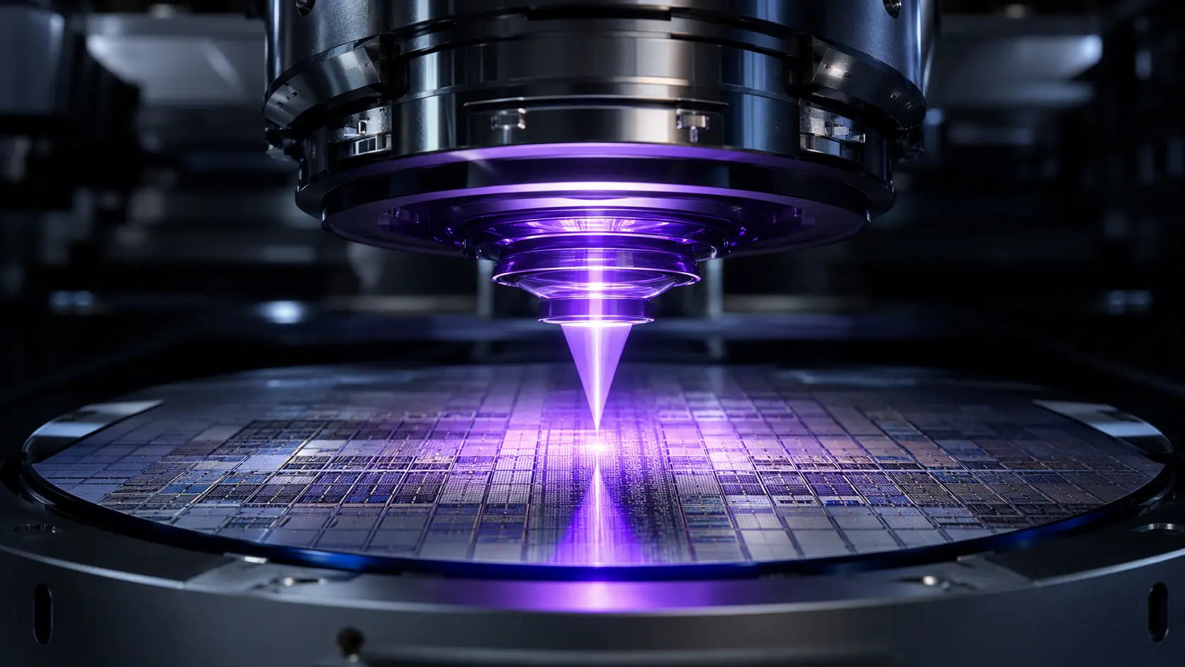
Extreme Ultraviolet (EUV) lithography prints the world’s most advanced microchips by bouncing 13.5-nanometer wavelength light off a reflective photomask. This photomask contains the physical blueprint of the microprocessor. The light reflects off the mask, travels through a series of reduction lenses, and strikes the raw silicon wafer.
Standard EUV systems possess a Numerical Aperture (NA) of 0.33. The light strikes the mask at a shallow 6-degree angle. Because the mask blueprint is formed by physically thick metallic absorbers, hitting it at an angle creates a microscopic shadow.
At the 0.33 NA scale, this shadow remains manageable. However, pushing silicon scaling below 2 nanometers requires capturing a wider cone of light, increasing the NA to 0.55. Physics dictates that absorbing this wider cone forces the light to strike the mask at a much steeper angle, dramatically elongating the shadow.
This elongated shadow completely ruins the projected circuit pattern. Engineers cannot simply make the metallic absorbers thinner, because the high-energy EUV light will bleed straight through them. The physical limits of geometric optics trap the entire semiconductor industry in a strict mathematical paradox.
ASML solved this geometry problem by inventing the anamorphic lens. Instead of projecting a symmetrical 4x reduction of the mask onto the silicon, the High-NA system applies asymmetric magnification.
It shrinks the pattern by 4x in the X-axis and 8x in the Y-axis. This distinct, uneven compression directly compensates for the specific angle of the incoming light, mathematically erasing the shadow and allowing the light to print flawless sub-2nm Angstrom-scale transistor gates.
WHY IT MATTERS NOW
The artificial intelligence hardware boom demands processor nodes operating at unprecedented densities. Printing these minute structures using legacy 0.33 NA machines requires double or triple patterning. Foundries must run the exact same wafer through a $200 million machine multiple times to print a single dense layer.
Multiple patterning destroys foundry economics. It dramatically increases the physical time it takes to process a wafer and introduces fatal alignment errors that crash yield rates. High-NA EUV restores single-patterning capability, directly rescuing the profit margins of leading foundries like TSMC and Intel.
However, the anamorphic solution carries a massive physical consequence. Standard EUV masks measure exactly 6 by 6 inches. Because the anamorphic lens shrinks the Y-axis by 8g instead of 4x, the final projected image on the silicon wafer is physically cut in half.
The absolute printing field drops from the legacy standard of 26mm x 33mm to a highly constrained 26mm x 16.5mm. This “half-field” restriction fundamentally breaks modern chip design. A monolithic AI accelerator like the Nvidia B200 already stretches the absolute physical limits of the standard 858-square-millimeter reticle limit.
A High-NA machine physically cannot print a chip of that size in a single flash. Consequently, the optical physics of the anamorphic lens forces the entire global computing ecosystem to abandon monolithic silicon designs. Companies must fracture their massive processors into smaller “chiplets” that fit inside the constrained High-NA half-field, fundamentally restructuring the advanced packaging supply chain.
WHAT MOST PEOPLE MISS
Semiconductor analysts widely assume the primary difficulty of High-NA EUV involves simply manufacturing larger, smoother Zeiss mirrors. They entirely miss the brutal kinematic reality of the half-field constraint.
Because the printable area is cut in half, the machine must physically scan the silicon wafer twice as fast to maintain baseline economic throughput. The mechanical stages holding the mask and the wafer must accelerate at $8\text{ g}$—nearly the physical limit of structural integrity—moving back and forth with sub-nanometer precision in a total vacuum. The true bottleneck is no longer just optics; it is the extreme mechanical acceleration required to feed the optics.
THE TRAJECTORY
Next 12–36 Months: Intel aggressively operationalizes the first High-NA EUV machines for its 14A node. The company absorbs the massive $350 million unit cost to secure early access to the anamorphic optics, attempting to leapfrog TSMC in geometric scaling capability.
Next Five Years: The complete standardization of advanced packaging architectures. Foundries will master “stitching”—the ability to print two separate half-field patterns flawlessly next to each other on the silicon. This will allow hardware manufacturers to digitally reconnect the fractured AI chips without losing interconnect bandwidth.
Next Ten Years: The ceiling of High-NA viability. As feature sizes shrink below 1 nanometer, extreme quantum tunneling will render physical silicon scaling obsolete. The industry will pivot toward Hyper-NA (0.75 NA) machines, requiring entirely new synthetic photomask materials to survive the highly concentrated radiation.
What Could Go Wrong: Photoresist sensitivity failure. The High-NA lens projects an image so small that standard chemical photoresists cannot absorb enough individual photons to reliably develop the pattern. This “shot noise” effect creates microscopic ragged edges on the transistors, destroying the electrical integrity of the entire wafer.
Most Likely Outcome: The anamorphic lens guarantees the continuation of Moore’s Law through the end of the decade. ASML will maintain absolute monopolistic control over the global computing roadmap, as no other entity on Earth possesses the engineering capacity to manipulate light at this extreme geometric asymmetry.
KEY TERMS
- High-NA EUV: An advanced lithography architecture that increases the numerical aperture of the optical system to 0.55 to print sub-2nm transistors.
- Anamorphic Lens: An optical system that provides different magnifications along different axes to distort or correct a projected image.
- Photomask: The physical, reflective template containing the precise geometric blueprint of the integrated circuit.
- Reticle Limit: The absolute maximum physical area of silicon that a lithography machine can expose in a single optical flash.
- Shot Noise: A statistical variance in the number of photons striking a specific area, causing fatal imperfections in microscopic silicon patterns.
SOURCES
- ASML — High-NA EUV Lithography: Architecture and Anamorphic Optics
- Carl Zeiss SMT — Optical Challenges and Solutions for 0.55 NA EUV Systems
- SPIE Digital Library — 3D Mask Effects and Shadowing Mitigation in High-NA EUV
- Institute of Electrical and Electronics Engineers (IEEE) — The Economics of Half-Field Reticles and Chiplet Integration