Advertisement
)

AT A GLANCE
- Concept: Isotropic Etching: A chemical gas reaction that removes material equally in all physical directions simultaneously.
- Concept: Sacrificial Layers: Temporary silicon-germanium structures built entirely to be destroyed later in the manufacturing sequence.
- Concept: Chemical Selectivity: The mathematical ratio dictating how fast the gas eats germanium versus pure silicon.
- Concept: Inner Spacers: Microscopic isolating walls inserted into the etched cavities to prevent catastrophic electrical short circuits.
HOW ISOTROPIC ETCHING WORKS
Building a modern Gate-All-Around (GAA) transistor requires suspending microscopic sheets of pure silicon in mid-air. Engineers achieve this impossible geometry through a process called epitaxial stacking. They grow alternating, ultra-thin layers of pure silicon and a sacrificial alloy known as silicon-germanium.
Once this semiconductor sandwich is standing, the foundry must remove only the silicon-germanium layers while leaving the pure silicon sheets perfectly intact. Standard plasma etching cannot execute this task. Traditional directional etching acts like a microscopic sandblaster, destroying everything in its vertical path.
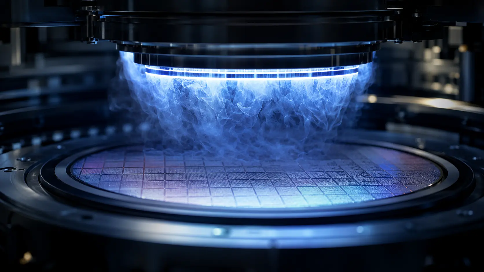
Instead, foundries deploy an isotropic chemical dry etch. They flood the wafer chamber with highly reactive, fluorine-based halide gases. Isotropic chemistry attacks the material from all angles simultaneously, creeping sideways into the exposed edges of the stacked crystal lattice.
The physics rely entirely on extreme chemical selectivity. The gas molecules react aggressively with the germanium atoms, converting the solid alloy into a volatile vapor that the chamber vacuums away. Because pure silicon lacks germanium, the chemical reaction mathematically stops the exact millisecond it hits the edge of the intended nanosheet channel, leaving the silicon suspended and undamaged.
WHY IT MATTERS NOW
The global semiconductor industry has officially exhausted the geometric limits of the FinFET transistor. Pushing silicon logic below the 3-nanometer threshold causes severe quantum tunneling, where electrons physically leak through the transistor gates. To maintain computational scaling, foundries must surround the entire silicon channel with the gate material to shut off this electrical leakage.
This physical transition makes Gate-All-Around the mandatory architecture for all future artificial intelligence and high-performance computing silicon. However, manufacturing a GAA transistor introduces an entirely new physical failure point known as the inner spacer cavity. After the initial isotropic etch carves out the silicon-germanium, engineers must insert dielectric insulating walls into those microscopic gaps.
If the isotropic etch removes too much material, the inner spacer becomes too thick, physically strangling the electrical current. If it removes too little, the spacer fails to insulate the gate, instantly short-circuiting the transistor. A variance of just three individual atoms completely destroys the chip.
This atomic-level precision dictates the financial survival of sovereign foundries. Samsung aggressively adopted GAA architecture early, betting its entire custom silicon business on mastering this exact etching step. TSMC delayed its GAA integration until its 2-nanometer node, prioritizing established yield margins over architectural first-mover advantage while it perfected its internal dry etch chemistry.
WHAT MOST PEOPLE MISS
Hardware reviewers frequently attribute generational chip performance gains simply to the new nanosheet shape. They entirely miss that the shape itself is purely a byproduct of advanced chemical fluid dynamics. A GAA transistor is fundamentally defined by the empty space left behind by the sacrificial layers.
The true engineering moat lies in managing extreme capillary forces during the etching process. If a foundry attempts to use a wet chemical bath instead of a dry gas etch, the physical surface tension of the liquid creates violent mechanical stress as the wafer dries. This microscopic fluid tension physically snaps the fragile, newly suspended silicon nanosheets, collapsing the entire transistor block and driving factory yield to zero.
THE TRAJECTORY
Next 12–36 Months: Major fabrication plants will ramp up their baseline 2nm GAA production lines. Foundries will heavily deploy specialized Atomic Layer Etching (ALE) tools that utilize self-limiting gas pulses, removing exactly one atomic layer of silicon-germanium per cycle to guarantee absolute dimensional uniformity across a 300mm wafer.
Next Five Years: The transition to highly stacked Complementary Field-Effect Transistors (CFET). Engineers will stack p-type and n-type nanosheets directly on top of each other vertically. This complex 3D integration will force chemical suppliers to engineer highly exotic, multi-stage isotropic gases capable of navigating microscopic vertical tunnels to reach deeply buried sacrificial layers.
Next Ten Years: The integration of two-dimensional transition metal dichalcogenides (TMDs). Silicon will reach its absolute physical exhaustion point. Foundries will transition to etching sacrificial layers surrounding molybdenum disulfide sheets just three atoms thick, requiring completely new halogen-free etching chemistries that do not spontaneously combust in the presence of exotic metals.
What Could Go Wrong: Severe wafer-edge non-uniformity. Gas distribution inside a vacuum chamber is rarely mathematically perfect. If the halide gas concentrates slightly heavier at the physical edge of the silicon wafer, the isotropic etch will carve those specific nanosheets a few atoms deeper than the chips in the center, silently wiping out twenty percent of a factory’s total profitable yield.
Most Likely Outcome: The isotropic dry etch will establish itself as the absolute master regulator of the sub-2nm era. Control over the exact atomic selectivity of semiconductor gases will heavily concentrate power among a few elite etching equipment manufacturers, making their intellectual property indispensable to global computing infrastructure.
KEY TERMS
- Gate-All-Around (GAA): A transistor architecture where the controlling gate material physically wraps around all four sides of the conductive silicon channel.
- Isotropic Etching: A chemical removal process that eats away target material uniformly in all physical directions at the exact same speed.
- Sacrificial Layer: A temporary structural material deposited during manufacturing specifically to be dissolved later to create microscopic cavities.
- Chemical Selectivity: The mathematical ratio that defines how much faster an etching gas destroys a target material compared to a protected adjacent material.
- Inner Spacer: A microscopic dielectric insulating wall inserted between the gate and the source-drain regions to prevent electrical short circuits.
SOURCES
- Applied Materials — Isotropic Dry Etching for Gate-All-Around Transistor Fabrication
- Institute of Electrical and Electronics Engineers (IEEE) — Inner Spacer Formation and Silicon-Germanium Selectivity in Nanosheet Architectures
- Lam Research — Atomic Layer Etching Mechanics and Advanced Semiconductor Scaling
- Journal of Vacuum Science & Technology — Highly Selective Isotropic Etching of SiGe over Si for Nanosheet Release