Advertisement
)
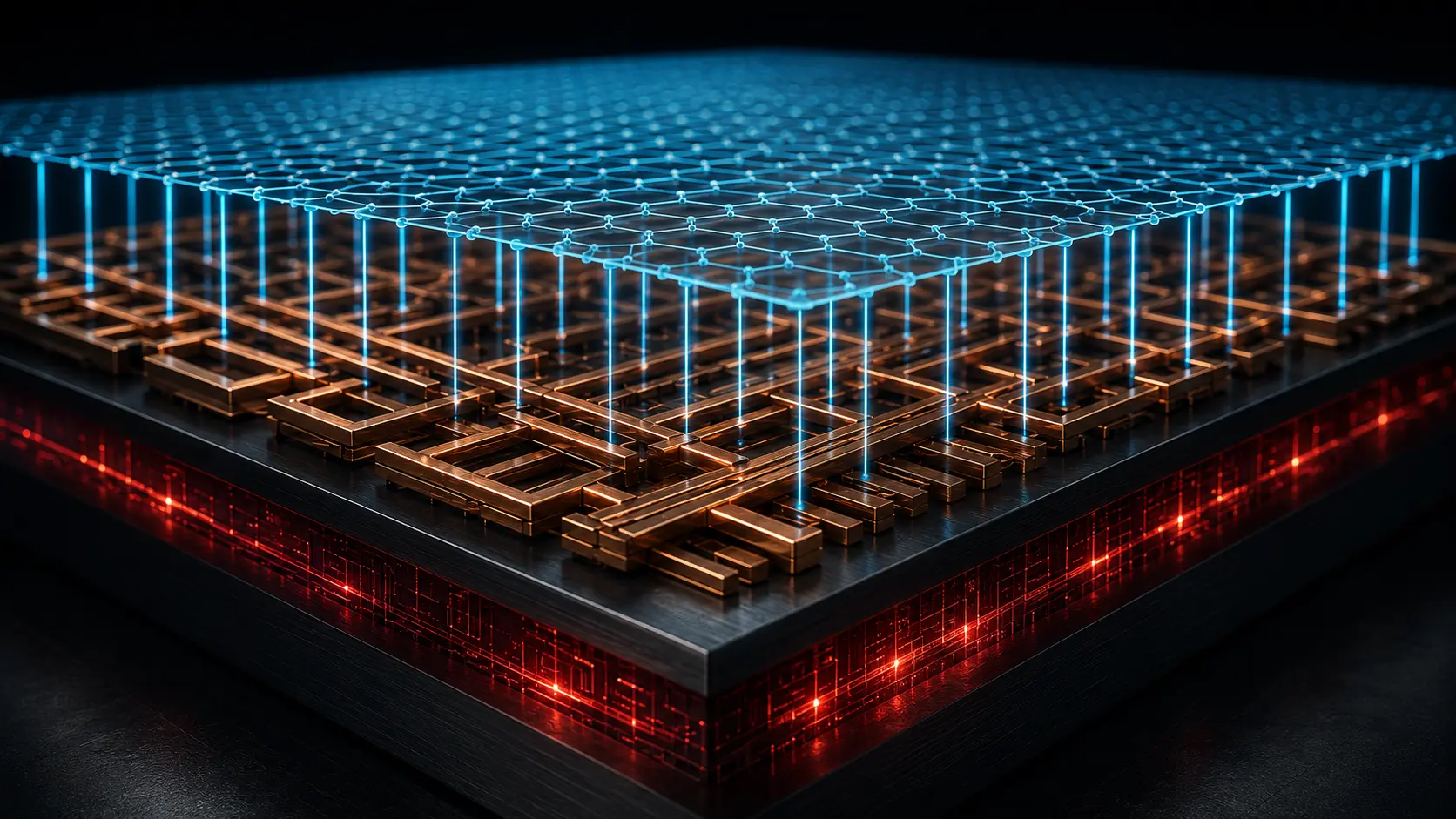

The semiconductor industry is running out of atoms. For fifty years, Moore’s Law was sustained by simply slicing silicon thinner and thinner, cramming more transistors onto a flat 2D chip. But physics has finally intervened. If you slice a piece of silicon thinner than a few nanometers, it stops acting like a solid wall. Quantum mechanics takes over, electrons leak uncontrollably through the material, and the chip generates catastrophic amounts of heat without doing any useful math. We have reached the physical limit of the silicon era; you cannot build the next generation of artificial intelligence on a foundation that is fundamentally melting.
Why should you care right now? Because the world’s most advanced laboratories are abandoning silicon. To keep computers scaling into the 2030s, engineers are turning to a radical new class of “2D materials” like Molybdenum Disulfide (MoS₂). These crystals are exactly one molecule thick and possess perfectly flat, flawless surfaces. More importantly, they can be printed directly on top of existing computer chips. Instead of building flat, sprawling, power-hungry processors, the tech industry is learning to stack these atomic sheets like floors in a skyscraper, unlocking a 10,000-fold increase in data speed and initiating the post-silicon era of global computing.
What are Monolithic 3D ICs with 2D Materials?
Monolithic 3D Integrated Circuits (ICs) are microchips built by sequentially printing layers of transistors directly on top of one another. By utilizing 2D materials like Molybdenum Disulfide (MoS₂) instead of silicon, manufacturers can bypass extreme heat limits, synthesizing ultra-thin, high-performance transistors directly over delicate copper wiring without melting the underlying circuitry.
At a Glance
- Concept: Instead of stacking completed, thick silicon chips like Legos, you use chemistry to print microscopic, atom-thin transistors directly onto the roof of an existing chip.
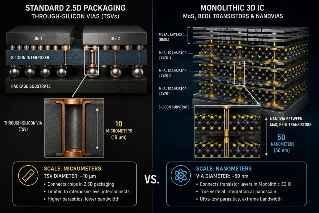
- Why it matters: Standard 3D stacking uses microscopic copper pillars (TSVs) that are relatively massive and spaced far apart. Monolithic 3D allows the top chip and bottom chip to connect at the exact scale of a transistor, drastically accelerating how fast memory feeds the AI brain.
- Who uses it: Mega-foundries (TSMC, Intel, Samsung) and global research institutes like IMEC are leading the fundamental materials science.
- Biggest takeaway: You can’t print silicon on top of a finished chip because making silicon requires 1,000°C heat, which would melt the chip below it. MoS₂ is the savior because it can be placed at low temperatures, respecting the “thermal budget.”
In Simple Words
Imagine a sprawling, one-story city (a Standard Silicon Chip). Everyone lives on the ground floor. As the city grows, people have to commute further and further to get to work, causing massive traffic jams and burning immense amounts of fuel (electricity and heat).
To solve this, we want to build skyscrapers. The old way of doing this (2.5D Packaging / TSVs) was to build a second city entirely separately, pick it up with a giant crane, drop it on top of the first city, and drill a few massive elevator shafts to connect them. It is better, but the elevators are still a bottleneck.
Monolithic 3D is like building the second floor directly on top of the first floor’s ceiling, connecting every single living room directly to the office above it via billions of tiny staircases. However, pouring traditional concrete (Silicon) requires a roaring fire that would burn the first floor down. Using 2D Materials like MoS₂ is like discovering a magical, ultra-strong, atom-thin building material that can be laid down completely cold, allowing us to build a 100-story skyscraper without ever damaging the ground floor.
Why This Matters
For Semiconductor Engineers, Hardware VCs, and Tech Analysts, Monolithic 3D is the ultimate endgame for AI memory bandwidth.
Currently, AI processors (like GPUs) and High-Bandwidth Memory (HBM) are built separately and placed side-by-side on a silicon interposer. Moving data horizontally across this bridge consumes massive amounts of power (picojoules per bit). If you can build the SRAM memory array monolithically—directly on top of the logic transistors using MoS₂—the distance the data travels shrinks from millimeters to nanometers. This architectural shift theoretically slashes AI power consumption by 90% while increasing bandwidth by orders of magnitude, completely resetting the competitive hierarchy of the global hardware market.
The Shift from FEOL to BEOL Transistor Integration
The semiconductor industry refers to the transistors at the bottom of a chip as the Front-End-Of-Line (FEOL). The delicate, microscopic copper wires built above them to route the electricity are the Back-End-Of-Line (BEOL).
For 50 years, active transistors were strictly confined to the FEOL. The BEOL was just dumb copper plumbing. Monolithic 3D with 2D materials fundamentally shatters this boundary. By placing active, switching transistors into the upper wiring layers, the chip becomes a living, three-dimensional neural volume. It stops being a flat grid of switches and becomes an integrated block of computational matter, mirroring the 3D density of the biological human brain.
How MoS2 Enables Monolithic 3D ICs
Replacing the most successful material in human history (silicon) requires exploiting the exotic physics of quantum confinement. Here is the first-principles breakdown of the architecture.
1. The Fundamental Problem: Short Channel Effects
In a transistor, a “Gate” controls the flow of electrons through a “Channel.” As we shrink transistors, the Gate gets too close to the source, and loses control. Electrons leak through the Channel even when the Gate is turned off. To stop this leakage, we must make the Channel material extremely thin (Extremely Thin Body – ETB electrostatics).
2. The Insufficiency of Silicon
If you slice silicon down to 1 nanometer to create an ETB, the physical surface of the silicon becomes chaotic. The “dangling bonds” (unattached silicon atoms) on the surface severely scatter the electrons trying to pass through, plunging the electrical mobility (speed) to useless levels. Silicon fails at the atomic scale.
3. The Core Mechanism: Transition Metal Dichalcogenides (TMDs)
Enter 2D materials like Molybdenum Disulfide (MoS₂). A layer of MoS₂ consists of a plane of Molybdenum atoms sandwiched between two planes of Sulfur atoms.
Unlike silicon, a sheet of MoS₂ is fully self-contained. It is held together by weak van der Waals forces, meaning it has zero dangling bonds on its surface. Electrons can glide through a 0.65-nanometer sheet of MoS₂ completely unbothered by surface scattering. It provides perfect electrostatic gate control with high carrier mobility.
4. Technical Depth: The BEOL Thermal Budget
To achieve Monolithic 3D, we must build the MoS₂ transistor in the BEOL, right on top of the delicate copper wires and low-k dielectric insulators of the first chip layer.
Copper melts and diffuses rapidly at high heat. Therefore, the Thermal Budget for any BEOL process is strictly capped at ~400°C. You cannot deposit high-quality silicon at 400°C. However, MoS₂ can be synthesized via low-temperature Metal-Organic Chemical Vapor Deposition (MOCVD) or physically transferred from a separate donor wafer at room temperature.
5. Real-World Consequences: Nano-Scale Vias
Because the MoS₂ layer is printed using standard lithography rather than stacked using a robotic arm, the vertical connections (vias) between the bottom silicon layer and the top MoS₂ layer can be as small as 50 nanometers. This is vastly smaller than the 10-micrometer Through-Silicon Vias (TSVs) used in today’s advanced packaging, unlocking interconnect densities of over 100 million vias per square millimeter.
Commercial Deployments: Monolithic SRAM and Edge AI
While Monolithic 3D with 2D materials is in the advanced R&D phase, its target applications dictate the future roadmaps of hyperscalers.
Monolithic SRAM Over Logic: The immediate target is memory. Currently, massive portions of an AI processor’s silicon real estate are consumed by SRAM (cache memory). By moving the SRAM entirely into the BEOL using MoS₂ transistors, chip designers free up 50% of the base silicon layer. They can fill this newly empty space with pure logic (math cores), effectively doubling the computing power of the chip without increasing its physical footprint.
Ultra-High-Density Edge AI: Small, battery-powered devices (like AR glasses or autonomous micro-drones) cannot afford the energy required to move data off-chip to separate memory modules. Monolithic 3D allows the creation of a “Compute-in-Memory” architecture. By stacking the 2D transistors directly over the sensors and memory, the chip can process visual data instantly on the exact same vertical axis, reducing power consumption to the milliwatt range.
Monolithic Image Sensors: Modern smartphone cameras already stack a pixel layer on top of a logic layer. By transitioning to a Monolithic 3D architecture using 2D materials, camera manufacturers can embed complex, pixel-level machine learning processing directly behind every individual photoreceptor, enabling real-time, zero-latency image enhancement and object recognition before the data ever reaches the phone’s main processor.
Economic & Strategic Impact
The transition to 2D materials will trigger a violent restructuring of the Semiconductor Equipment Supply Chain.
For decades, the industry relied on companies like ASML for extreme ultraviolet (EUV) lithography to shrink silicon in 2D. While lithography remains critical, Monolithic 3D shifts immense economic value toward deposition and materials engineering. Companies specializing in Atomic Layer Deposition (ALD), Chemical Vapor Deposition (CVD), and advanced wafer-bonding techniques (like Applied Materials and Tokyo Electron) will capture massive new revenue streams. The geopolitical advantage will shift toward nations and consortiums that control the intellectual property for synthesizing defect-free MoS₂ and Tungsten Diselenide (WSe₂) at 300mm wafer scales.
Advantages
- Ultimate Interconnect Density: Monolithic vias are thousands of times smaller than TSVs, removing the data-transfer bottleneck that currently limits Artificial Intelligence.
- Immunity to Short Channel Effects: The ultra-thin, flawless van der Waals surface of 2D materials allows for extreme scaling without the catastrophic electron leakage seen in silicon.
- Thermal Budget Compliance: 2D materials can be integrated directly into the BEOL without exceeding the 400°C limit, protecting the delicate copper wiring underneath.
- Heterogeneous Integration: Allows engineers to mix and match different 2D materials in vertical layers—for instance, an N-type MoS₂ layer on top of a P-type WSe₂ layer—creating highly optimized 3D logic gates.
Limitations
- Synthesis Defects: Currently, growing a large, 300mm wafer of MoS₂ often results in “grain boundaries”—microscopic cracks where the crystal structures don’t perfectly align. These defects trap electrons and ruin the performance of the transistor.
- Contact Resistance: Connecting a 3D metal wire to a 2D, one-atom-thick sheet is chemically agonizing. The high “contact resistance” at this junction currently burns up much of the electrical performance gained by using the 2D material.
- P-Type Material Scarcity: While MoS₂ is excellent for N-type (electron-conducting) transistors, building a complete computer requires P-type (hole-conducting) transistors. Finding and synthesizing a stable, matching 2D P-type material (like Tungsten Diselenide) with equal performance remains a significant materials science challenge.
Common Misconceptions
Misconception: 2D materials are a completely new way of doing math.
Reality: The logic is exactly the same (1s and 0s). We are still building standard Field Effect Transistors (FETs). The only difference is the material the channel is made of. It is an upgrade to the physical plumbing, not a change to the software.
Misconception: Monolithic 3D replaces advanced packaging like TSMC’s CoWoS.
Reality: They are complementary, operating at completely different physical scales. CoWoS connects massive, finished chips together at the millimeter scale. Monolithic 3D builds transistors inside a single chip at the nanometer scale. Future AI will use both simultaneously.
Misconception: Silicon will go extinct.
Reality: Silicon will remain the undisputed king of the base layer (FEOL). The bottom foundation of the skyscraper will always be heavy, highly optimized silicon. The 2D materials are specifically used for the upper floors (BEOL) where silicon cannot safely be poured.
What Most People Miss
The disruptive potential of Layer Transfer Techniques.
Most analysts assume that to build Monolithic 3D, the MoS₂ must be chemically grown directly on the delicate copper BEOL, forcing the agonizing 400°C thermal limit constraint.
What many miss is the rapid advancement of “Wafer-to-Wafer Transfer.” Instead of growing the 2D material on the fragile chip, scientists grow the perfect MoS₂ crystal on a separate, blank “donor” wafer at a scorching 1,000°C to ensure flawless quality. Then, using temporary adhesives and precise mechanical peeling, they literally peel the 1-atom-thick layer off the donor wafer like a sticker, and press it gently onto the cold BEOL of the actual chip. If the industry perfects this transfer process, it bypasses the thermal budget constraint entirely, accelerating the commercialization timeline of Monolithic 3D by a decade.
Comparison Table
| Feature | FinFET / GAA (Standard Silicon) | 2.5D / 3D Packaging (TSVs) | Monolithic 3D (2D Materials) |
| Material | Silicon | Silicon | MoS₂ / TMDs (over Silicon) |
| Integration Level | 2D / Horizontal | Chip-to-Chip | Transistor-to-Transistor |
| Vertical Connection Size | N/A | Massive (10 – 50 µm) | Microscopic (50 nm) |
| Thermal Budget | > 1000°C (FEOL) | 250°C (Soldering) | < 400°C (BEOL Synthesis) |
| Dangling Bonds | Severe at sub-2nm | Severe | Zero (van der Waals) |
Case Study
Situation: As global foundries mapped their technology nodes past 1 nanometer (the angstrom era), they faced the physical impossibility of continuing to shrink silicon channels without triggering catastrophic subthreshold leakage. Furthermore, routing power and data to these densely packed 2D chips was choking the interconnect layers.
Challenge: Prove that active transistors could be relocated from the silicon base into the upper wiring layers to create a true 3D compute volume, without destroying the underlying circuitry.
Solution (IMEC 2D BEOL Demonstrations): The premier semiconductor research institute, IMEC, aggressively pivoted to 2D materials. They initiated programs to evaluate the integration of MoS₂ into standard 300mm wafer fabrication flows. To overcome the thermal budget of the Back-End-Of-Line, IMEC optimized low-temperature Metal-Organic Chemical Vapor Deposition (MOCVD) and explored advanced layer-transfer methodologies to integrate 2D channels directly above traditional copper interconnects.
Outcome: IMEC successfully demonstrated fully functional MoS₂ transistors manufactured on 300mm wafers utilizing BEOL-compatible processes. While the contact resistance and defect densities still lagged behind mature silicon, the proof-of-concept verified that double-gated 2D transistors could successfully operate in the upper wiring layers of a chip.
Lessons Learned: The milestone proved that the post-silicon transition is not merely a theoretical physics problem, but a highly actionable engineering roadmap. It validated that the multi-billion-dollar semiconductor equipment market must rapidly pivot its R&D toward atomic layer transfer and low-temperature transition metal synthesis if it hopes to supply the foundries of the 2030s.
Future Outlook
Next 12–24 Months
The era of Defect Mitigation and Contact Resistance Engineering. In the immediate term, the industry will remain locked in intense laboratory R&D. Foundries like TSMC and Intel will heavily fund academic partnerships to solve the high contact resistance at the source/drain junctions of MoS₂ transistors. Semi-equipment providers (Applied Materials, TEL) will introduce the first commercial-grade 300mm deposition and transfer tools explicitly designed for 2D materials, transitioning the physics from bespoke flakes of tape (exfoliation) into scalable, automated wafer processes.
Next 3–5 Years
The scaling of SRAM BEOL Prototypes. By the late 2020s, we will see the first commercial prototype chips featuring true Monolithic 3D integration. These will not be main logic processors; they will be specialized memory architectures. Foundries will demonstrate working silicon chips featuring functional MoS₂-based SRAM caches built directly in the BEOL wiring layers. This hybrid architecture will serve as the commercial beachhead, proving that memory bandwidth can be vastly expanded without increasing the physical 2D footprint of the die.
Next 10 Years
The Post-Silicon Volume Transition. By the mid-2030s, the limits of standard Gate-All-Around (GAA) silicon nanosheets will be fully exhausted. Monolithic 3D ICs using stacked layers of Transition Metal Dichalcogenides will enter High-Volume Manufacturing (HVM). These ultra-dense, skyscraper-like microchips will dominate the artificial intelligence and high-performance computing (HPC) markets. They will execute logic, store memory, and process optical data seamlessly across perfectly aligned vertical layers, achieving a compute density that permanently secures the continuation of Moore’s Law well into the 21st century.
Most Likely Scenario
Silicon will never be fully abandoned, but its role will be fundamentally demoted to the basement of the microchip. The future of computational scaling relies entirely on mastering the chemistry of 2D atomic crystals. The foundries that successfully commercialize the low-temperature integration of MoS₂ into the BEOL will achieve an insurmountable architectural advantage, dictating the physical speed limit of the global AI economy.
Key Takeaways
- Monolithic 3D ICs involve printing new, active transistors directly on top of the copper wiring of an existing chip, creating a dense, vertical “skyscraper” of computing power.
- Silicon cannot be used for this because creating silicon requires 1,000°C heat, which would melt and destroy the delicate copper wiring underneath.
- The solution relies on 2D materials like Molybdenum Disulfide ((MoS₂)), which are exactly one atom thick and can be deposited or transferred at low, safe temperatures.
- Unlike silicon, 2D materials lack “dangling bonds” on their surface. This allows electrons to flow through them perfectly even when the material is sliced to sub-nanometer thicknesses.
- Moving memory (SRAM) into these upper 3D layers drastically shortens the distance data must travel, saving immense amounts of power and shattering the memory bandwidth bottleneck in AI.
- The primary challenge is manufacturing: seamlessly printing massive, 300mm sheets of MoS₂ without microscopic tears or high electrical resistance remains intensely difficult.
Glossary
Back-End-Of-Line (BEOL): The upper layers of a microchip consisting of delicate copper wires and insulators that route electricity between the transistors. It has a strict maximum thermal budget of roughly 400°C.
Carrier Mobility: A measurement of how quickly and easily an electron can move through a semiconductor material. High mobility means a faster, cooler chip.
Contact Resistance: The electrical friction that occurs when a 3D metal wire tries to connect to a 1-atom-thick 2D material. Currently, it is a major performance bottleneck for MoS₂.
Extremely Thin Body (ETB): A transistor design where the conductive channel is sliced incredibly thin to prevent electrons from leaking through when the transistor is turned off.
Front-End-Of-Line (FEOL): The very bottom layer of a microchip where the actual, active silicon transistors are formed at extreme temperatures.
Transition Metal Dichalcogenide (TMD): A class of 2D materials (like MoS₂ or WSe₂) that form ultra-thin, perfectly flat planes held together by weak van der Waals forces, possessing excellent semiconducting properties.
Sources
Nature: Two-dimensional materials for next-generation computing technologies
IMEC: 2D materials: the next logical step in semiconductor scaling
IEEE Spectrum: Monolithic 3D Integration: The Ultimate Scaling for Moore’s Law
TSMC Symposium / Research: Low-Temperature Growth of 2D Materials for BEOL Integration
Applied Physics Reviews: Integration of 2D materials for monolithic 3D ICs