Advertisement
)

AT A GLANCE
- Concept: Physical Trace Attenuation: High-frequency electrical signals degrade rapidly when crossing physical circuit board pathways.
- Concept: Four-Level Signaling: PAM4 packs two bits per cycle into four distinct voltage amplitudes.
- Concept: Bit Error Rate: Increased voltage levels lower structural noise margins, requiring aggressive digital error fixes.
- Concept: Chiplet Bottlenecks: Physical interface distances limit data speeds between modular silicon processing tiles.
HOW IT WORKS
Modern artificial intelligence accelerators outgrow the physical size limits of single silicon wafers. To increase processing density, manufacturers divide a single massive processor into a cluster of smaller, specialized modular tiles called chiplets. These separate tiles must exchange vast amounts of data across packaging substrates with near-zero latency.
The Peripheral Component Interconnect Express (PCIe) bus provides the standardized electrical pathways that connect these disparate silicon structures. To double data throughput without increasing the physical operating frequency, PCIe Generation 6 introduces Pulse Amplitude Modulation 4 (PAM4) signaling. This methodology replaces traditional binary on-off voltages with four distinct electrical amplitude levels.
By utilizing four separate voltage levels, each signal pulse transmits two bits of information simultaneously ($00$, $01$, $10$, $11$). This expansion presents a severe physical challenge because the voltage gap between each state shrinks by two-thirds. This narrow window exposes the signal to extreme interference from localized thermal noise and physical trace attenuation.
As high-frequency electrical pulses travel across copper lines and package substrates, the high-frequency components fade faster than low-frequency components. This asymmetric degradation causes the signal pulses to smear into one another, a physical phenomenon known as inter-symbol interference. To combat the resulting spike in the Bit Error Rate (BER), the interconnect architecture deploys a hardware-level Forward Error Correction (FEC) engine alongside a low-latency cyclic redundancy check to reconstruct damaged data packets instantly before they reach the processing core.

WHY IT MATTERS NOW
The physical scaling limits of traditional monolithic silicon chips are slowing down global compute advancements. Shrinking transistors down to sub-2nm nodes yields diminishing returns due to soaring manufacturing costs and quantum tunneling defects. Consequently, semiconductor giants are shifting their capital expenditures toward advanced heterogeneous packaging solutions.
Software tools developed by market leaders like Synopsys and Cadence now focus heavily on verifying signal integrity at the physical trace layout level rather than optimizing individual chip logic. The ultimate performance of an AI data center no longer depends solely on raw floating-point operations. It depends directly on the bandwidth limits of the bus infrastructure connecting those processors.
This infrastructure shift underpins the design of next-generation hardware platforms like multi-die architectures and advanced graphics processing arrays. These massive computing systems combine dozens of compute and memory chiplets on a single organic substrate. Without highly optimized PCIe interconnect channels, the individual silicon units spend excessive processing cycles idling while waiting for data transfers to complete.
Geopolitically, controlling the intellectual property of high-speed interconnect standards dictates computing sovereignty. The PCI Special Interest Group (PCI-SIG) sets these open international standards, turning the licensing of compliant physical-layer designs into a critical bottleneck for domestic chip initiatives. Nations building localized semiconductor industries must master these optoelectronic and electrical trace physics to field competitive high-performance computing clusters.
WHAT MOST PEOPLE MISS
Most computing analysts evaluate system speed by tracking the aggregate bandwidth numbers advertised in trade brochures. They treat the interconnect as an invisible, friction-free straw that gulps data effortlessly between chip boundaries. They overlook the intense power tax imposed by the error correction loops required to keep those high-speed buses stable.
As the system pushes data across physical board traces, the Forward Error Correction engine consumes significant amounts of power just to analyze and clean up noisy PAM4 signals. This process creates an engineering paradox: maximizing interconnect bandwidth generates a thermal load that can throttle the adjacent processing cores. The real design triumph is not hitting raw peak bandwidth, but configuring the trace geometry to minimize physical attenuation, allowing the error-correction systems to run in low-power states.
THE TRAJECTORY
Next 12–36 Months: Broad commercial adoption of PCIe Gen 6 will reshape enterprise data center motherboard designs. System architects will switch from cheap FR4 circuit board materials to expensive, ultra-low-loss substrates to preserve signal integrity across expanded distances.
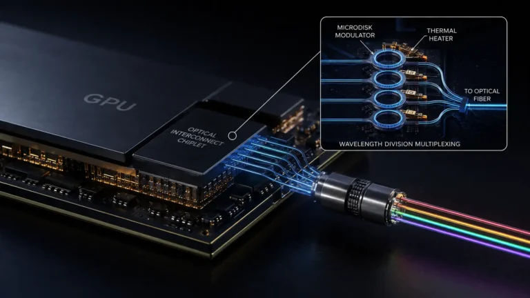
Next Five Years: Optical PCIe links will enter high-end AI clusters to replace copper traces entirely for multi-meter distances. Transceiver modules will connect directly to chiplet packages, using modulated light waves to eliminate physical trace attenuation and radically lower data-transit power demands.
Next Ten Years: Unified, open-standard chiplet ecosystems will allow engineers to mix and match silicon blocks from completely different foundries on a single substrate. The interconnect layer will act as a universal plug-and-play fabric, transforming hardware manufacturing into a modular assembly process.
What Could Go Wrong: If the latency overhead of Forward Error Correction engines surpasses acceptable limits for real-time parallel computing, the scaling of multi-chiplet clusters will plateau. System architects would be forced to abandon PAM4 signaling and return to wider, power-hungry parallel buses, inflating manufacturing costs.
Most Likely Outcome: The computing landscape will see complete architectural dominance by software-defined interconnect layers. Physical trace configurations will be tightly integrated with predictive error-correction algorithms, ensuring stable performance variations even as underlying silicon blocks push against material limits.
KEY TERMS
- Pulse Amplitude Modulation 4 (PAM4): A signaling technology that maps two bits of data onto four separate voltage levels within a single clock cycle.
- Bit Error Rate (BER): The percentage of transmitted data bits that arrive corrupted due to noise, interference, or signal degradation.
- Forward Error Correction (FEC): A hardware-level error-control method that injects redundant data into a signal path to let the receiver fix errors without retransmission.
- Trace Attenuation: The loss of signal strength and clarity that occurs as high-frequency electrical pulses travel through a physical transmission medium like copper.
- Chiplet: An independent, specialized integrated circuit block designed to be combined with other modular tiles on a single unified package substrate.
SOURCES
- PCI-SIG — PCI Express Base Specification Revision 6.0
- Synopsys Technical Repository — Overcoming Signal Attenuation and Noise Barriers in PAM4 PCIe 6.0 Implementations
- Cadence Design Systems — Physical Layer Validation and Bit Error Rate Optimization for Heterogeneous Chiplet Architectures
- IEEE Transactions on Very Large Scale Integration (VLSI) Systems — Latency and Thermal Optimization of Forward Error Correction in Advanced Interconnects