Advertisement
)

Artificial intelligence is burning the physical world to the ground. Today’s cutting-edge AI models are trained on massive clusters of Graphics Processing Units (GPUs), which perform trillions of calculations by pushing electrons through microscopic silicon wires. This brute-force movement of electricity creates a fatal byproduct: heat. We are rapidly approaching the thermal and electrical limits of modern data centers, where simply cooling the processors consumes nearly as much energy as running them. To scale the next generation of AI, the hardware industry must stop fighting electrical resistance.
Why should you care right now? Because semiconductor engineers are replacing the electron with the photon. Instead of pushing electricity through copper, a new breed of computer chips performs the heavy mathematics of artificial intelligence by intersecting beams of light. By transferring data and executing matrix multiplication entirely within the optical domain, these chips calculate at the physical speed of light with near-zero thermal dissipation. Photonic Neural Networks are poised to bypass the physical limitations of Moore’s Law, fundamentally redefining the speed, scale, and energy economics of global AI infrastructure.
What are Photonic Neural Networks?
Photonic Neural Networks are advanced hardware architectures that execute artificial intelligence computations directly using light. By leveraging photonic integrated circuits, they utilize optical interference and wavelength-division multiplexing to perform matrix multiplication at the speed of light, achieving sub-nanosecond latency and extreme energy efficiency compared to traditional electronic processors.
At a Glance
- Concept: Building a computer chip out of microscopic glass channels (waveguides) instead of copper wires, using lasers to do the math instead of electricity.
- Why it matters: Electronic chips generate massive heat and latency because electrons bump into atoms (resistance). Photons (light) have no mass and do not experience electrical resistance, allowing for calculations that use a fraction of a picojoule of energy.
- Who uses it: Hyperscale cloud providers, algorithmic high-frequency trading firms, and leading photonic hardware startups (e.g., Lightmatter, Celestial AI, Lightelligence).
- Biggest takeaway: Photonics offers extreme parallelism. You can send ten different colors of light down the exact same microscopic optical wire at the exact same time, performing ten different AI calculations simultaneously without them mixing.
In Simple Words
An artificial intelligence model is essentially a giant machine that does multiplication and addition over and over again.
In a standard computer chip, to multiply 2 by 3, the chip sends a burst of electricity (electrons) through a microscopic wire. The electricity physically hits a transistor, turns it on, and spits out an answer. Pushing billions of electrons through tiny wires causes friction, which creates massive amounts of heat. This is why your laptop gets hot when it runs a heavy program.
A Photonic Neural Network completely changes the medium. Instead of electricity, it uses light.
Imagine shining two flashlights at each other so their beams cross. When light waves intersect, they interfere with each other, creating a new, combined wave. Photonic chips use microscopic, on-chip lasers to shoot beams of light through tiny glass tunnels. By carefully crossing these light beams, the physical intersection of the light automatically calculates the math problem instantly. Because light has no mass and travels at 186,000 miles per second, the calculation happens in a fraction of a nanosecond, and because there is no electrical friction, the chip stays completely cold.
Why This Matters
The enterprise deployment of Generative AI is currently bottlenecked by the “Memory Wall” and data movement latency. Moving data from an electronic memory chip to an electronic processor requires immense energy and time.
For Hardware Engineers, Cloud Architects, and AI Investors, photonic computing represents a structural leap. It unlocks “sub-nanosecond” inference latency. For financial institutions running AI to execute algorithmic trades, or autonomous vehicles parsing high-definition LiDAR feeds to avoid a collision, traditional GPU latency (measured in milliseconds) is too slow. Photonic Tensor Cores process this imagery literally at the speed of light, establishing an entirely new performance frontier where computing delay is dictated by the speed of light in silicon, not the switching speed of a transistor.
The Rise of Optical Neural Networks in AI
The photonic computing landscape in the mid-2020s is driven by the convergence of telecommunications optics and semiconductor lithography.
For decades, the telecom industry used optical fibers to move data across oceans. However, when that optical data reached a server, it hit an Optical-Electrical-Optical (OEO) conversion bottleneck. The light had to be converted into electricity, processed by a CPU, and converted back into light to be sent out again. This OEO conversion is incredibly slow and wastes massive power.
The breakthrough of Photonic Neural Networks is keeping the data as light during the actual computation. By migrating the optical components directly onto the silicon wafer (Silicon Photonics), companies are building integrated circuits where the entire neural network inference occurs purely in the optical domain, bypassing the OEO conversion tax entirely.
How Photonic Neural Networks Work
Performing deterministic mathematical operations using waves of light requires hacking the physics of optical interference. Here is the first-principles breakdown of the architecture.
1. The Fundamental Problem: The MAC Bottleneck
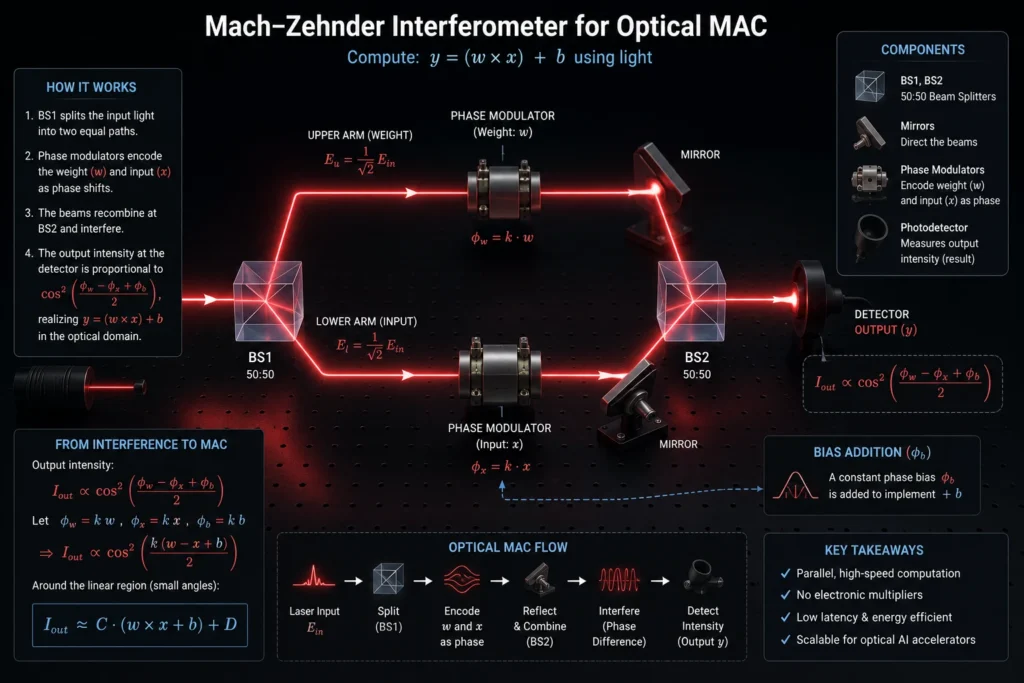
The core of every neural network is the Multiply-Accumulate (MAC) operation, mathematically expressed as finding the dot product of vectors:
Y = W * X + B
In modern Large Language Models (LLMs), executing a single prompt requires trillions of these MAC operations. Electronic GPUs perform these sequentially or via limited parallel clusters, facing hard limits on how fast transistors can open and close.
2. The Insufficiency of Electrons
As we shrink transistors below 2 nanometers, the copper interconnects between them become so thin that electrical resistance skyrockets. The electrons suffer from Resistance-Capacitance (RC) delay, meaning the chip cannot run any faster without melting the silicon.
3. The Core Mechanism: Mach-Zehnder Interferometers (MZIs)
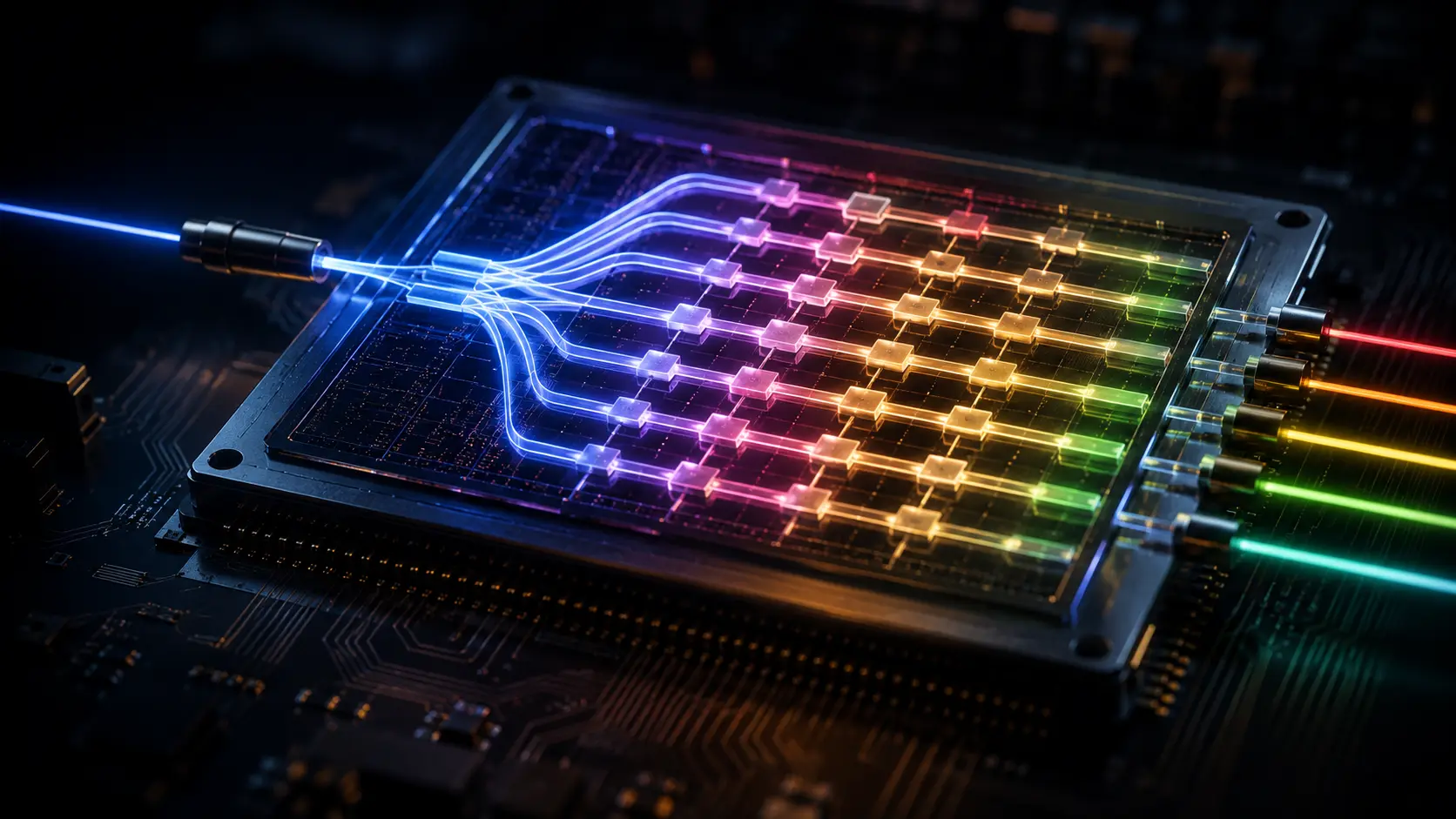
Photonic chips perform MAC operations using a grid of microscopic optical components called Mach-Zehnder Interferometers (MZIs).
An MZI takes an incoming beam of light (the input data, X) and splits it down two separate microscopic paths. On one of the paths, a tiny heater or electro-optic modulator applies a “phase shift” to the light wave. This phase shift represents the neural network’s learned “Weight” (W).
4. Technical Depth: Optical Interference
When the two paths recombine at the end of the MZI, the light waves physically interfere with each other. If the waves are perfectly aligned (in-phase), they combine to make a brighter light. If they are misaligned (out-of-phase), they cancel each other out, making a dimmer light. The brightness of the exiting light is the exact mathematical product of the input multiplied by the weight. An entire layer of a neural network can be physically constructed by chaining together a massive mesh of these MZIs.
5. Real-World Consequences: Wavelength-Division Multiplexing (WDM)
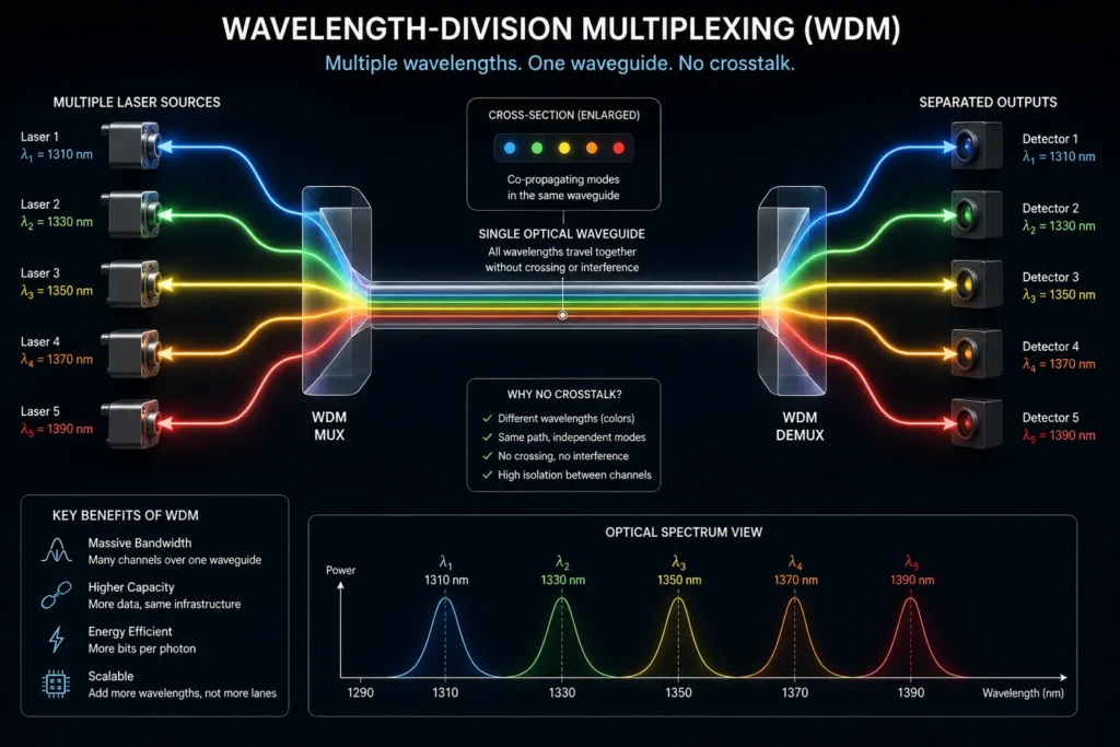
Photonic Tensor Cores exploit a property of physics that electrons cannot: Wavelength-Division Multiplexing (WDM).
You cannot push two electrical signals down the same copper wire without them scrambling each other. However, you can shoot a red laser and a blue laser down the exact same optical waveguide simultaneously, and they will simply pass right through each other. By using different colors of light, a photonic chip can process massive, multi-dimensional matrices in parallel on the exact same physical footprint, exponentially increasing the compute density per square millimeter.
Commercial Applications of Photonic Computing
Photonic computing is migrating from the laboratory physics bench into aggressive commercial deployments where latency is paramount.
High-Frequency Algorithmic Trading: In the financial sector, moving a trade order one microsecond faster than a competitor generates millions in arbitrage profit. Financial firms are deploying photonic accelerators because optical inference models calculate market risk directly at the speed of light. Because the data propagates through the chip physically rather than waiting for discrete electronic clock cycles, the latency overhead is virtually eliminated.
Autonomous Vehicle Perception Systems: Driving a car at highway speeds requires real-time, zero-latency processing of high-definition camera and LiDAR feeds. Traditional GPUs suffer from memory bandwidth bottlenecks when ingesting this massive sensory data. Photonic tensor cores can process massive 3D point-cloud arrays simultaneously via WDM, providing the vehicle’s “brain” with instantaneous object recognition and obstacle avoidance logic.
Telecommunications and Edge AI: 5G and 6G cellular networks generate astronomical amounts of signal data. By embedding photonic neural networks directly into cell tower base stations, telecom providers can execute AI-driven signal routing and noise cancellation directly in the optical domain before the data is ever converted into electricity, drastically reducing the thermal footprint of edge infrastructure.
Economic & Strategic Impact
The core strategic challenge for the industry is the Hybrid Packaging Bottleneck.
While matrix multiplication is easy to do with light, neural networks also require “Nonlinear Activation Functions” (like the ReLU or Sigmoid functions) to make complex, non-linear decisions. Creating an “all-optical” nonlinear activation function is currently extremely difficult and inefficient.
Therefore, modern commercial photonic chips are Hybrid Processors. The optical domain performs the heavy, fast matrix multiplication, but the light is then captured by a photodetector, converted back to electricity, and handed to a standard digital transistor to perform the nonlinear activation and memory retrieval. For semiconductor supply chains, this requires “Co-Packaged Optics” (CPO)—the ability to seamlessly fuse delicate optical glass components and standard silicon transistors onto the exact same microscopic die without them destroying each other. Mastering this hybrid packaging is the definitive moat for hardware companies in the late 2020s.
Advantages
- Sub-Nanosecond Latency: Computations occur as light propagates through the medium, eliminating the clock-cycle delays of electronic processors and delivering instantaneous inference.
- Sub-Picojoule Energy Efficiency: Because photons do not suffer from electrical resistance, the energy required per MAC operation is a fraction of traditional GPUs, drastically lowering data center cooling and power costs.
- Massive Parallelism (WDM): Multiple independent calculations can be executed in the exact same physical space simultaneously simply by using lasers of different wavelengths (colors).
Limitations
- Nonlinear Computations: Truly efficient, all-optical nonlinear activation functions do not yet exist at commercial scale, forcing the architecture to rely on hybrid optical-electrical conversions that re-introduce slight latency and power penalties.
- Lack of Optical Memory: You cannot easily “store” a photon in place. Because light must keep moving, photonic chips lack a native, high-density optical Random Access Memory (RAM), forcing them to constantly fetch data from slower electronic memory banks.
- Manufacturing Immaturity: Fabricating thousands of perfectly calibrated Mach-Zehnder Interferometers requires absolute microscopic precision. The slightest manufacturing defect or thermal expansion in the silicon can misalign the lasers, degrading the accuracy of the neural network.
Common Misconceptions
Misconception: Photonic chips will replace all CPUs and GPUs.
Reality: Photonic chips are incredibly specialized “Domain-Specific Accelerators.” They are brilliant at the dense matrix multiplication required for AI, but they are terrible at general-purpose computing (like running an operating system, word processor, or database). They will sit alongside standard CPUs, not replace them.
Misconception: The entire computer runs on light.
Reality: Only the AI math engine runs on light. The data storage, the motherboard, the control logic, and the memory still operate entirely on standard electrical electrons.
Misconception: Photonic chips use visible, glowing lasers like a sci-fi movie.
Reality: Silicon photonics typically operates using near-infrared light (often around the 1550 nm wavelength, the standard for telecommunications). This light is completely invisible to the human eye.
What Most People Miss
The disruptive threat to Digital Precision Expectations.
Standard electronic GPUs operate digitally (using 1s and 0s), which guarantees absolute mathematical precision. If a GPU calculates 2 x 2, the answer is always exactly 4.
What most people miss is that Photonic Neural Networks are Analog Computers. They calculate math by measuring the physical brightness of a continuous light wave. If a microscopic temperature fluctuation changes the glass waveguide slightly, the output might be 3.99 or 4.01. While this slight analog “noise” would crash a traditional banking database, neural networks are remarkably resilient. AI models inherently thrive on probabilities and approximations. The industry is betting that the slight loss in mathematical precision is vastly outweighed by the 100x improvement in speed and energy efficiency.
Comparison Table
| Feature | Electronic GPU (NVIDIA Hopper/Blackwell) | Photonic Tensor Core (Hybrid PNN) |
| Information Carrier | Electrons | Photons (Light) |
| Primary Limitation | RC Delay, Massive Heat Generation | Optical-Electrical Conversion, Memory |
| Computation Speed | Bound by Transistor Clock Cycles | Physical Speed of Light Propagation |
| Parallelism Method | Spatially separate transistor cores | Wavelength-Division Multiplexing (WDM) |
| Energy per MAC | High (measured in picojoules) | Ultra-low (sub-picojoule range) |
| Calculation Type | Digital (Exact precision) | Analog (Approximate light intensity) |
Case Study
Situation: As Large Language Models crossed the trillion-parameter threshold, hyperscale cloud providers faced an existential power crisis. Training and running inference on massive electronic GPU clusters consumed gigawatts of power, pushing facilities beyond the thermal limits of their municipal electrical grids.
Challenge: Achieving higher compute density without increasing the thermal footprint. The core bottleneck was the energy cost of simply moving data between the High-Bandwidth Memory (HBM) and the compute cores, alongside the intense heat of the MAC operations themselves.
Solution (The Hybrid Photonic Accelerator): Startups like Lightmatter introduced hybrid photonic-electronic platforms (such as the Envise architecture). By replacing the electronic tensor cores with a massive mesh of Mach-Zehnder Interferometers, the platform shifted the heavy matrix multiplication entirely into the optical domain.
Outcome: The photonic accelerator demonstrated the ability to execute neural network inference with an energy efficiency vastly superior to legacy silicon. By executing operations in parallel via WDM and calculating at the speed of light, the architecture achieved a dramatic reduction in both latency and total thermal output, proving that the physical limitations of Moore’s Law could be bypassed by changing the physics of the carrier particle.
Lessons Learned: The implementation confirmed that the future of AI hardware is hybrid. It proved that while electrons remain superior for memory storage and logical control flow, photons are the undisputed, mathematically superior medium for executing the dense, parallel matrix mathematics required by modern deep learning.
Future Outlook
Next 12–24 Months
The era of Optical I/O and Co-Packaged Optics (CPO). Before full photonic neural networks take over data centers, the immediate transition will focus on data movement. Over the next two years, hyperscalers will aggressively replace the copper wires connecting GPUs to each other with Optical I/O chiplets. By building lasers directly into the GPU packaging (CPO), chips will be able to share memory and talk to each other across the data center at the speed of light, solving the immediate interconnect bottleneck plaguing distributed AI training.
Next 3–5 Years
The scaling of Commercial Hybrid Inference Engines. By the end of the decade, rack-mounted hybrid photonic accelerators will reach widespread commercial maturity. These server blades will be specifically deployed for AI inference tasks (running the models, rather than training them). In highly latency-sensitive environments—such as global financial exchanges, autonomous drone routing, and real-time biometric video analysis—photonic tensor cores will become the mandatory baseline infrastructure.
Next 10 Years
The pursuit of All-Optical Neural Networks (ONNs). By the mid-2030s, the field will attempt to eliminate the electron entirely from the AI pipeline. Breakthroughs in novel metamaterials and phase-change materials will yield highly efficient, purely optical nonlinear activation functions and optical memory arrays. When data can enter a chip as light, be multiplied as light, activate as light, and be stored as light without ever touching a copper wire, humanity will achieve the absolute theoretical apex of computational energy efficiency.
Most Likely Scenario
Photonic Neural Networks will not kill the traditional silicon GPU; they will absorb it. The data center of 2030 will rely on an intricate symbiosis: electronic systems for memory and logic management, seamlessly wrapped around a photonic core that silently, instantly, and coldly crunches the trillion-parameter matrices driving global artificial intelligence.
Key Takeaways
- Photonic Neural Networks use beams of laser light instead of electricity to perform the heavy mathematics (matrix multiplication) required by artificial intelligence.
- Because light has no mass, it does not create the electrical resistance (heat) that is currently choking traditional electronic GPU data centers.
- The math is physically calculated using a Mach-Zehnder Interferometer (MZI), a microscopic glass channel that splits light, shifts its phase (the weight), and recombines it to create a mathematical interference pattern.
- Through Wavelength-Division Multiplexing (WDM), a photonic chip can shoot multiple different colors of light through the same wire simultaneously, calculating massively parallel arrays without cross-talk.
- Current systems are “Hybrid.” They use light for the fast, heavy math, but convert the light back to electricity to handle nonlinear activation functions and memory access.
- Photonic chips act as analog computers; they trade absolute digital precision for sub-nanosecond latency and sub-picojoule energy efficiency.
Glossary
Mach-Zehnder Interferometer (MZI): The foundational optical component of a photonic chip. It splits a light beam, alters the phase of one path, and recombines them, using the resulting interference to physically calculate a mathematical multiplication.
Multiply-Accumulate (MAC) Operation: The core mathematical equation of artificial intelligence (Y = W * X + B). It involves multiplying an input by a weight and adding it to an accumulator.
Optical-Electrical-Optical (OEO) Conversion: The slow, energy-wasting process of turning a light signal into an electrical signal so a computer can process it, and then turning it back into light. Photonic computing aims to bypass this entirely.
Phase Shift: Altering the timing of a light wave. In photonic computing, changing the phase shift of a laser beam is how the system encodes the “weight” of the neural network.
Photonic Integrated Circuit (PIC): A microchip that processes light (photons) instead of electricity (electrons), using microscopic glass waveguides instead of copper wires.
Wavelength-Division Multiplexing (WDM): A technique that allows multiple different frequencies (colors) of laser light to travel down the same optical path simultaneously, enabling extreme parallel computation.
Frequently Asked Questions
Are photonic chips faster than quantum computers?
They serve entirely different purposes. Quantum computers use quantum mechanics (superposition/entanglement) to solve specific, highly complex mathematical problems (like breaking cryptography or simulating molecules). Photonic chips are designed to do standard, classical AI math (matrix multiplication), but they do it at the absolute maximum physical speed allowed by the universe.
If they run on light, do they work in the dark?
Yes. The light is generated entirely internally by microscopic, on-chip lasers (often Vertical-Cavity Surface-Emitting Lasers, or VCSELs). They do not rely on external ambient light or sunlight.
Why don’t we have these in our smartphones yet?
Scaling down optical components is difficult. While transistors can be shrunk to 2 nanometers, photons have a specific physical wavelength (e.g., 1550 nm). You cannot shrink an optical waveguide smaller than the wavelength of the light it carries, meaning photonic chips are currently physically larger than electronic chips and better suited for massive data centers than mobile phones.
Are they really 100% heat-free?
No. While the optical calculation itself generates near-zero heat, the onboard lasers that generate the light produce heat, and the electrical components required for the hybrid memory/control logic also produce heat. However, the total thermal footprint is a fraction of a comparable electronic GPU.
Can I run standard Python code on a photonic chip?
Yes, from the developer’s perspective. Companies building these chips provide compiler software that takes standard AI models written in PyTorch or TensorFlow and automatically translates them into the optical phase-shift instructions required by the hardware.
Sources
- Journal of Lightwave Technology: Photonic Neural Networks: Principles, Progress, and Prospects Toward Streaming Processes (August 2026)
- Patsnap Insights: Photonic neuromorphic computing landscape 2026 (April 2026)
- Patsnap Eureka: Photonic Tensor Cores vs GPUs: Latency Comparison in AI Workloads (May 2026)
- Vividcomm: Unlocking AI’s Future: The Rise of Optical Neural Networks (November 2025)
- Medium / Tim Ventura: Photonic Computing: Can AI Move at the Speed of Light? (May 2026)