Advertisement
)

If you want to build a highly efficient electric vehicle or a megawatt-scale solar grid, traditional silicon microchips will fail you. When subjected to the massive voltages and extreme heat of modern power systems, standard silicon physically melts or short-circuits. To handle this immense power, the global automotive and energy sectors have pivoted to a radically superior material: Silicon Carbide (SiC). By switching from silicon to SiC, an electric vehicle instantly gains 10% more range, charges drastically faster, and sheds hundreds of pounds of cooling equipment.
However, there is a catastrophic bottleneck in the supply chain. You cannot simply mass-produce Silicon Carbide like standard silicon. While a traditional silicon crystal the size of an adult human can be pulled from a vat of liquid metal in a few days, growing a piece of Silicon Carbide the size of a hockey puck takes weeks inside an intensely specialized, 2,500°C furnace. If the temperature fluctuates by a fraction of a degree during those weeks, microscopic defects form inside the crystal, permanently ruining the microchips that will eventually be cut from it. Why should you care right now? Because the geopolitical race for electrification is entirely dependent on mastering the dark art of SiC crystal growth. The companies that can grow these flawless synthetic crystals at scale will effectively control the hardware infrastructure of the 21st-century energy transition.
What is Silicon Carbide (SiC) Boule Growth?
Silicon Carbide (SiC) boule growth is the metallurgical process of synthesizing a raw, cylindrical SiC crystal (a boule) from which semiconductor wafers are sliced. Because SiC does not melt, it is grown via Physical Vapor Transport (PVT), where solid SiC powder is vaporized at extreme temperatures and slowly condensed onto a cooler seed crystal over several weeks.
At a Glance
- Concept: Growing synthetic, wide-bandgap semiconductor crystals by vaporizing powder at half the temperature of the surface of the sun.
- Why it matters: SiC chips handle 10x the voltage of standard silicon, making them mandatory for EV traction inverters and grid-level transformers. The shortage of defect-free SiC wafers dictates the production limits of the entire EV industry.
- Who uses it: Elite semiconductor manufacturers (Wolfspeed, Infineon, STMicroelectronics, Onsemi) and automotive giants (Tesla, BYD, Porsche).
- Biggest takeaway: Standard silicon is a commodity; SiC substrates are a highly guarded proprietary technology. The recipe for controlling the temperature gradients inside a SiC furnace is fiercely protected trade secret, representing the ultimate barrier to entry in the power electronics market.
In Simple Words
Making a traditional silicon microchip is like making a popsicle. You melt the ingredients into a liquid, dip a stick in, and pull out a perfectly formed, solid structure. It is fast, reliable, and cheap.
Making a Silicon Carbide (SiC) microchip is completely different because SiC stubbornly refuses to melt into a liquid. If you heat it up, it just turns directly from a solid into a gas.
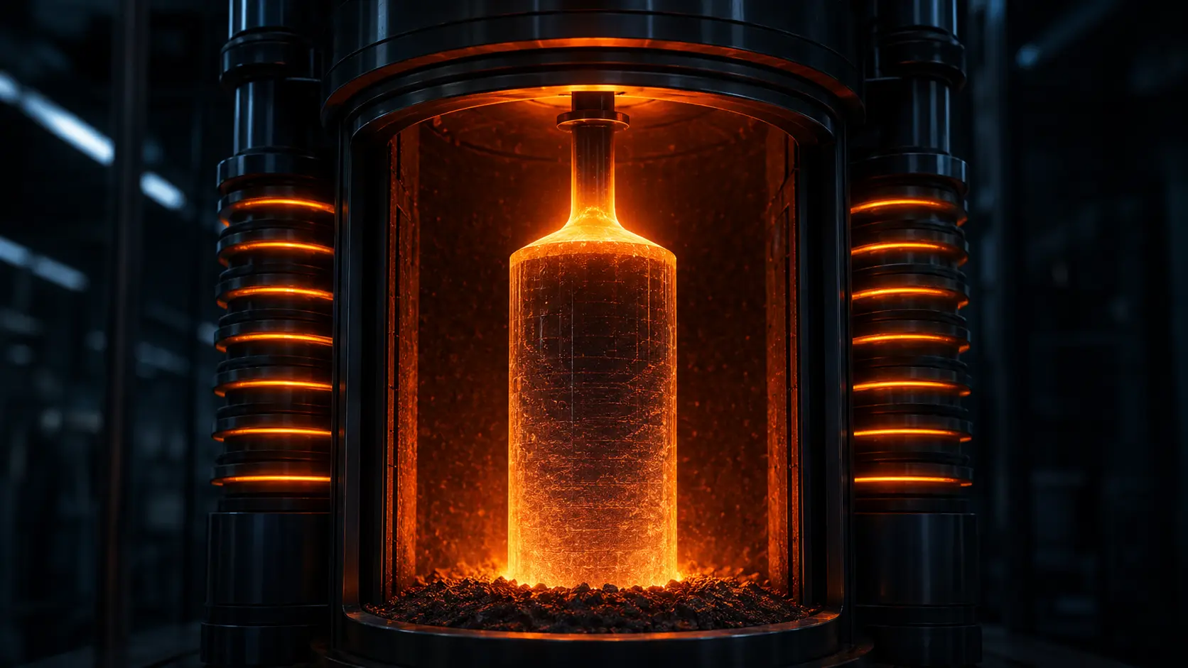
Therefore, growing a SiC crystal is like trying to grow a massive, flawless diamond using steam. Manufacturers put raw SiC powder at the bottom of a furnace and a tiny “seed” crystal at the top. They heat the bottom to an astonishing 2,500°C. The powder turns into a gas, floats up to the slightly cooler top of the furnace, and perfectly sticks to the seed. This gas has to stack atom by atom, layer by layer, for weeks, to build a cylinder of raw material (the boule). If a single atom falls out of place during those weeks, a microscopic crack forms. When you slice that cylinder into flat wafers to make chips, that tiny crack will cause the final microchip to explode when exposed to the high voltage of an electric car battery.
Why This Matters
The semiconductor industry is uniquely bifurcated. For advanced logic chips (like the NVIDIA GPUs running artificial intelligence), the bottleneck is the lithography—the extreme ultraviolet (EUV) lasers required to etch microscopic circuits onto the silicon. The raw silicon wafer itself is cheap and abundant.
For power electronics, the exact opposite is true. The etching process is relatively old and simplistic, but the raw material is astronomically expensive and scarce. A raw, unetched 150mm (6-inch) SiC wafer can cost over $1,000, compared to less than $50 for a standard silicon wafer.
For Supply Chain Executives and Hardware Buyers, this completely alters procurement strategies. You cannot simply design a brilliant SiC chip and hire a foundry to print a million of them. You must secure long-term, multi-billion-dollar supply agreements specifically for the raw substrates. The companies that physically grow the boules—not the companies that etch the circuits—wield the ultimate pricing power in the electrification supply chain.
The Transition to 200mm Silicon Carbide Wafers
The global transition from 150mm (6-inch) to 200mm (8-inch) SiC wafers is the most critical macroeconomic event in the power semiconductor industry.
When you slice a cylindrical boule into flat wafers, a 200mm wafer yields almost twice as many usable chips as a 150mm wafer. This economy of scale is required to drive down the cost of electric vehicles. However, increasing the diameter of a SiC boule by just two inches fundamentally breaks the thermodynamics of the furnace.
As the boule grows wider, the temperature differences between the center of the crystal and the outer edges become harder to control. This thermal stress causes the crystal lattice to warp, generating massive defect densities at the edges of the 200mm wafer. Overcoming this thermal warping is the multi-billion dollar hurdle that companies like Wolfspeed and Coherent are currently fighting to clear.
How Silicon Carbide (SiC) Boule Growth Works
Creating a flawless, wide-bandgap crystal lattice requires manipulating thermodynamics in an environment where no human can physically observe the process. Here is the first-principles breakdown.
1. The Fundamental Problem: The Absence of a Liquid Phase
To grow a flawless crystal, the easiest method is to pull a seed slowly from a liquid melt (the Czochralski process), which allows the atoms to align perfectly. Silicon Carbide does not have a liquid phase at atmospheric pressures; it sublimates directly from solid to vapor. This forces the industry to rely on vapor deposition.
2. The Insufficiency of Chemical Vapor Deposition (CVD)
CVD is used to grow microscopic, thin films of materials, but it is vastly too slow to grow a massive, thick cylinder (a boule) required for bulk wafer manufacturing. A more aggressive, bulk-growth method is required.
3. The Core Mechanism: Physical Vapor Transport (PVT)
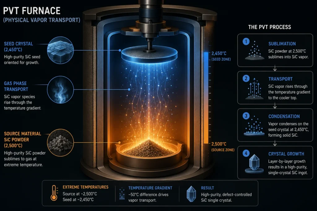
The industry standard is PVT. Inside a graphite crucible, raw silicon and carbon powder are placed at the bottom. A high-quality SiC “seed” crystal is mounted at the top. The crucible is placed inside a highly insulated furnace and heated via induction coils.
4. Technical Depth: Sublimation and the Thermal Gradient
The bottom of the crucible is heated to approximately 2,500°C, vaporizing the powder into a cloud of silicon and carbon gas. The top of the crucible (where the seed is located) is kept slightly cooler, exactly 2,450°C. This precise 50°C thermal gradient forces the vapor to drift upward and condense onto the seed crystal. The crystal grows at a painstakingly slow rate of roughly 0.1 to 0.5 millimeters per hour.
5. Real-World Consequences: Defect Propagation
Because the growth takes weeks and relies entirely on gas condensing into a solid, the crystal lattice is highly susceptible to stress. If the temperature gradient shifts, or if the graphite crucible degrades slightly, structural defects form.
- Basal Plane Dislocations (BPDs): Misalignments in the crystal planes that propagate outward.
- Threading Screw Dislocations (TSDs): Microscopic, spiral-staircase disruptions in the lattice.When the boule is finally sliced into thin wafers, these defects are physically embedded in the substrate. If a chip manufacturer etches a high-voltage transistor directly on top of a BPD, the transistor will fail, destroying the yield of the entire production run.
Applications of SiC Power Electronics
The excruciatingly slow growth of SiC boules directly dictates the deployment speed of next-generation infrastructure.
Electric Vehicle Traction Inverters: This is the primary driver of the SiC market. The traction inverter converts the DC power from the battery into AC power for the electric motor. Traditional silicon inverters lose massive amounts of energy as heat during this conversion. SiC inverters operate with near-perfect efficiency, extending the vehicle’s range by 10% and allowing the car to utilize 800-volt architectures for ultra-fast charging (as seen in the Porsche Taycan and Hyundai platforms).
Solid-State Grid Transformers: Standard utility transformers on the power grid are massive, oil-filled metal boxes that have not changed fundamentally in a century. SiC substrates allow engineers to build Solid-State Transformers (SSTs)—compact, fully digital power routers that are a fraction of the size and weight of legacy transformers, seamlessly managing the bidirectional power flow between massive solar farms, battery arrays, and the municipal grid.
High-Speed Rail and Light Rail: Modern high-speed train networks require immense power conversion within tight weight constraints. SiC power modules drastically reduce the size and cooling requirements of the train’s traction systems, directly lowering the overall weight of the train and significantly reducing the massive energy required to accelerate the locomotive to 300 km/h.
Economic & Strategic Impact
Because the raw substrate is so expensive and difficult to grow, the SiC industry operates on a strict Vertical Integration Model.
In the standard silicon world, companies like AMD or Apple design a chip (fabless) and pay TSMC to manufacture it. The supply chain is highly segmented.
In the Silicon Carbide world, segmentation is economically suicidal. If a company only designs the chip and buys the raw SiC wafers from a third party, they operate at the absolute mercy of the substrate supplier. Therefore, companies like Wolfspeed, STMicroelectronics, and Onsemi have vertically integrated. They own the PVT furnaces to grow the boules, the diamond wire saws to slice the wafers, and the cleanrooms to etch the circuits. This massive capital intensity creates an impenetrable economic moat; a new startup cannot simply enter the SiC market without spending billions of dollars and a decade mastering basic thermodynamic metallurgy.
Advantages (of SiC over Silicon)
- Wide Bandgap: SiC has a bandgap of ~3.26 eV compared to standard silicon’s 1.12 eV. This allows SiC chips to withstand voltages 10x higher before the semiconductor breaks down and shorts out.
- Thermal Conductivity: SiC conducts heat almost three times better than silicon. It pulls heat away from the circuit so efficiently that automakers can completely eliminate bulky, heavy liquid cooling loops from their inverters.
- High Switching Frequency: SiC transistors can turn on and off at drastically higher frequencies with near-zero switching losses, allowing engineers to shrink the size of the heavy copper coils and capacitors required in the surrounding power system.
Limitations (of the Manufacturing Process)
- Abysmal Growth Speed: While silicon boules grow at speeds measured in millimeters per minute, SiC boules grow at millimeters per hour. A furnace can only produce a few inches of material after weeks of continuous, high-energy operation.
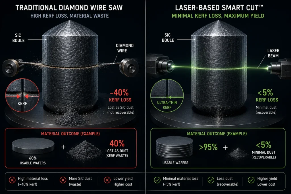
- The Slicing Bottleneck: SiC is the third hardest material on Earth, trailing only diamonds and boron carbide. Slicing the tough, raw boule into thin wafers requires specialized diamond-impregnated wire saws. The cutting process is incredibly slow, wears out the expensive diamond wire rapidly, and completely grinds nearly 40% of the precious crystal into worthless dust (kerf loss).
- The Seed Crystal Paradox: To grow a SiC boule via PVT, you must start with a perfect SiC seed crystal. But to get a perfect SiC seed crystal, you have to grow a perfect SiC boule. If a manufacturer’s seed inventory has microscopic defects, those defects will perfectly replicate and multiply in every new boule they grow, making it exceptionally difficult for new competitors to synthesize clean material from scratch.
Common Misconceptions
Misconception: We can solve the shortage by just building more furnaces.
Reality: Furnaces are not the bottleneck; operational knowledge is. The exact temperature gradients, pressure levels, and crucible designs required to grow a flawless boule without cracking it are highly guarded trade secrets. Simply buying a furnace does not mean you know how to operate it at a commercial yield.
Misconception: SiC is a brand-new material.
Reality: Silicon Carbide (historically known as Carborundum) has been used as industrial sandpaper and abrasive grinding powder since the 1890s. What is new is the ability to synthesize it into a perfectly ordered, continuous, single-crystal lattice suitable for microelectronics.
Misconception: The entire microchip is made of Silicon Carbide.
Reality: The substrate (the foundation) is made of SiC. However, chipmakers still use a process called “epitaxy” to grow a thin, perfectly pure active layer of SiC on top of the sliced wafer, which is where the actual microscopic transistor circuitry is etched.
What Most People Miss
The disruptive potential of Smart Cut and Cold Split Technologies.
Because growing the boule takes weeks and slicing it wastes 40% of the material as dust, the industry is desperately trying to bypass traditional diamond wire saws.
What most people miss is the massive R&D flowing into laser and ion-cleaving technologies. Companies like Soitec (SmartCut) and Infineon (Cold Split) are pioneering methods where lasers or hydrogen ions are fired exactly 300 micrometers deep into the solid boule. This creates a microscopic plane of weakness inside the crystal. Engineers then apply rapid thermal shock (cold and heat) to literally snap a perfect, razor-thin wafer off the top of the boule without using a saw. This completely eliminates the 40% dust waste, theoretically allowing manufacturers to instantly double the number of wafers they extract from a single, painstakingly grown crystal.
Comparison Table
| Feature | Standard Silicon (Si) | Silicon Carbide (SiC) | Gallium Nitride (GaN) |
| Growth Method | Czochralski (Liquid Melt) | Physical Vapor Transport (Sublimation) | Vapor Deposition on foreign substrates |
| Bandgap Energy | 1.12 eV | 3.26 eV (Wide Bandgap) | 3.4 eV (Wide Bandgap) |
| Wafer Cost (Estimate) | < $50 | $800 – $1,200+ | Variable (Often grown on cheap Silicon) |
| High-Voltage Tolerance | Low (< 600V efficiency limit) | Extreme (800V to 3,300V+) | Moderate to High (Best < 1,000V) |
| Primary Use Case | Logic (CPUs/GPUs), Low Power | Heavy Power (EVs, Grid, Rail) | Fast Switching (Chargers, RF, LiDAR) |
Case Study
Situation: The global automotive industry recognized that shifting EVs from 400-volt to 800-volt architectures was mandatory to achieve sub-20-minute fast charging. However, legacy silicon Insulated-Gate Bipolar Transistors (IGBTs) could not handle the 800V loads without suffering massive efficiency losses, forcing the industry to adopt SiC MOSFETs.
Challenge: The sudden, overwhelming demand for SiC chips created an immediate supply chain crisis. Foundries could not produce enough chips because the raw 150mm (6-inch) SiC substrates were too scarce, too expensive, and prone to microscopic basal plane dislocations that ruined the final automotive-grade circuits.
Solution (The 200mm Transition): Wolfspeed, holding massive institutional knowledge in crystal growth, executed a highly aggressive, multi-billion-dollar pivot to 200mm (8-inch) wafers, opening the Mohawk Valley Fab in New York—the world’s first fully automated 200mm SiC facility.
Outcome: Scaling the boule growth from 150mm to 200mm was a thermodynamic nightmare, requiring years to stabilize the temperature gradients to prevent the larger crystals from warping at the edges. However, once stabilized, the 200mm wafers yielded nearly 1.8x more usable chips per wafer.
Lessons Learned: The case study proved that achieving dominance in the power electronics market requires relentless vertical integration. The ability to successfully synthesize and slice massive, 200mm defect-free boules immediately locked in multi-billion-dollar supply agreements with OEMs like Jaguar Land Rover and Lucid Motors, proving that substrate metallurgy, not just circuit design, is the ultimate gatekeeper of the EV revolution.
Future Outlook
Next 12–24 Months
The era of Automotive Qualification Bottlenecks. As dozens of Chinese material suppliers (like SICC and TankeBlue) rapidly scale their own PVT furnaces to break the Western monopoly, the market will flood with raw SiC substrates. However, automotive-grade chips require near-zero defect densities. Over the next two years, we will see a severe divergence: cheap, lower-quality SiC wafers will saturate the industrial and solar inverter markets, while flawless, high-yield wafers required for life-critical EV drivetrains will remain highly constrained and fiercely expensive.
Next 3–5 Years
The mass adoption of Laser Slicing and Wafer Bonding. By the late 2020s, the traditional diamond wire saw will be largely phased out for SiC production. The integration of laser-cleaving technologies will drastically reduce kerf loss, instantly doubling the output of the existing furnace fleet. Furthermore, companies will perfect “wafer bonding”—taking a highly defective, cheap SiC substrate and bonding a microscopic, flawless layer of premium SiC purely on the surface. This will drastically crash the cost per wafer, fundamentally disrupting the pricing power of the legacy boule growers.
Next 10 Years
The Ultra-High Voltage Grid Transition. As SiC wafer costs plummet, the technology will expand beyond the 800V automotive market into the 3,300V to 10,000V+ utility market. SiC will replace the massive, mechanical substations that currently manage the municipal power grid. Solid-State Transformers built on 200mm SiC wafers will seamlessly and instantly route gigawatts of power between neighborhood solar grids, massive AI data centers, and offshore wind farms, permanently retiring the mechanical era of power transmission.
Most Likely Scenario
Silicon Carbide is the undisputed king of high-power electronics, but the agony of PVT boule growth will remain the industry’s ultimate constraint. The companies that figure out how to bypass the furnace—through laser splitting, advanced epitaxy, or engineered wafer bonding—will crash the cost of SiC from an exotic premium material down to a ubiquitous industrial commodity, unlocking the true scale of global electrification.
Key Takeaways
- Silicon Carbide (SiC) is mandatory for modern EVs and power grids because it can handle extreme voltages and heat that would instantly melt traditional silicon.
- Because SiC does not melt into a liquid, it must be grown from a gas using Physical Vapor Transport (PVT) inside a 2,500°C furnace.
- Growing a single SiC crystal (a boule) takes weeks and requires a flawless “seed” crystal. Any slight temperature shift creates fatal microscopic cracks (defects) in the lattice.
- Slicing the incredibly hard SiC boule into wafers uses diamond wire saws that grind 40% of the precious, time-consuming crystal into worthless dust.
- The industry is shifting from 150mm (6-inch) to 200mm (8-inch) wafers to produce more chips, but growing the wider crystals exponentially increases the risk of thermal warping and defects.
- Because the raw material is so hard to make, SiC chipmakers must vertically integrate (owning the furnaces, the saws, and the cleanrooms) to survive, creating a massive barrier to entry.
Glossary
Bandgap: The amount of energy required to knock an electron loose and create electrical flow. SiC is a “Wide Bandgap” material, meaning it requires massive energy to break down, allowing it to handle extreme voltages.
Basal Plane Dislocation (BPD): A microscopic, fatal defect in the crystal lattice that propagates horizontally. If an active transistor is printed over a BPD, it will eventually short circuit under high voltage.
Boule: A raw, unetched, cylindrical synthetic crystal (resembling a large hockey puck or log) that is eventually sliced horizontally into flat wafers.
Czochralski Method: The fast, standard method for making standard silicon, where a seed crystal is dipped into a vat of liquid, molten silicon and pulled upward. Impossible for SiC because it does not melt.
Kerf Loss: The amount of valuable crystal material that is completely wasted (ground into dust) by the physical thickness of the saw blade during the slicing process.
Physical Vapor Transport (PVT): A highly complex metallurgical process where a solid powder is heated until it vaporizes into a gas, drifts upward, and condenses back into a solid crystal on a cooler surface.
Frequently Asked Questions
Why don’t they just melt the Silicon Carbide?
It violates the laws of physics at standard pressures. Silicon Carbide sublimates—it turns directly from a solid powder into a gas when heated to extreme temperatures, completely bypassing the liquid phase.
Is Silicon Carbide better than Gallium Nitride (GaN)?
They serve different purposes. GaN is excellent for fast, lower-power switching (like your fast-charging laptop brick or LiDAR sensors). SiC is built for heavy, brute-force power (like the drivetrain of a 5,000-pound electric truck or a municipal power grid transformer).
How many microchips come from one boule?
A single SiC boule might be 20 to 30 millimeters thick. When sliced into thin wafers (each a fraction of a millimeter thick), a single boule might yield 30 to 40 wafers. Each wafer can then be etched to contain hundreds of individual microchips, depending on their size.
Why is it called the “Seed Crystal Paradox”?
You cannot grow a SiC crystal out of nothing; the gas needs a perfect template (a seed) to condense onto. But the only way to get a perfect seed is to slice the top off an already perfect, fully grown SiC boule. If you don’t already have one, it is incredibly difficult to start.
Can artificial intelligence speed up the furnace?
AI is being heavily deployed to monitor the acoustic and thermal emissions of the PVT furnaces to predict when a defect is forming. However, AI cannot change the fundamental thermodynamic physics of how fast the gas condenses onto the crystal lattice without warping it.
Sources
[1] IEEE Transactions on Electron Devices: Impact of Basal Plane Dislocations on the Reliability of SiC Power MOSFETs (2025/2026 Analysis)
[2] Wolfspeed, Inc.: The Transition to 200mm Silicon Carbide Manufacturing: Yields and Thermodynamics (Investor Briefings)
[3] Soitec: SmartSiC™ Technology: Overcoming Boule Slicing Waste with Advanced Wafer Bonding
[4] Yole Intelligence: Power SiC: Materials, Devices and Applications (2026 Market Report)
[5] Materials Science Forum: Physical Vapor Transport Growth of Bulk SiC Crystals: Challenges and Advances