Advertisement
)

AT A GLANCE
- Concept: Optical Interconnects: Using light pulses instead of electrical currents to move data between processors.
- Concept: Co-Packaged Optics (CPO): Fusing the laser components directly onto the same silicon substrate as the main processor.
- Concept: Wave-Division Multiplexing: Sending multiple colors of light down a single fiber to multiply data capacity.
- Concept: Signal Attenuation: The natural degradation of electrical signals as they travel through physical copper wires.
IN SIMPLE WORDS
Imagine trying to empty a massive swimming pool using a standard garden hose. No matter how much pressure you apply, the water can only flow so fast. This is the current state of modern computers.
Processors are incredibly fast, but they must send their data to other computers through copper wires. Pushing high-speed electricity through copper causes intense friction, generating heat and destroying the signal if it travels more than a few feet.
Silicon photonics fixes this physical traffic jam by changing the medium. Instead of pushing electricity through copper, engineers use microscopic lasers to encode the data into flashes of light. They shoot this light through tiny glass tubes called fiber optics. The data now travels at the speed of light with almost zero heat or friction, allowing giant warehouses of computers to instantly act as one massive, unified brain.
HOW SILICON PHOTONICS WORKS
For decades, the semiconductor industry relied on copper interconnects to move data between processors and memory banks. As data rates scale into terabits per second, copper hits an absolute physical wall. High-frequency electrical signals suffer from severe attenuation, meaning the signal literally dies as it travels down the wire.
To solve this, foundries manufacture optoelectronic transceivers. These devices sit at the edge of the server rack, converting outgoing electrical signals from the processor into optical pulses, and converting incoming light back into electricity.
The physical challenge is that pure silicon cannot generate light. It possesses an indirect bandgap, meaning it releases energy as heat, not photons. Engineers solve this by bonding distinct III-V semiconductor materials, such as Indium Phosphide, directly onto the silicon wafer to act as the laser source.
Once the laser generates a steady beam of light, the silicon chip uses microscopic structures called Mach-Zehnder modulators to chop the light beam into billions of digital pulses per second.
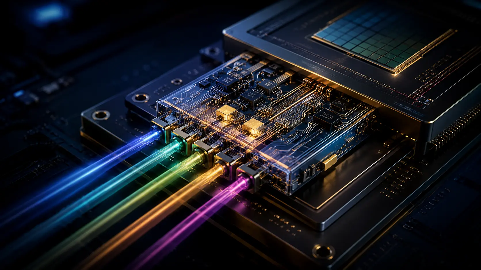
To maximize bandwidth, these chips employ Wave-Division Multiplexing (WDM). The system generates several different colors of light, encodes data onto each specific color, and combines them all into a single glass fiber. A prism-like structure on the receiving end separates the colors back out, massively multiplying the total data throughput without laying more physical cables.
Historically, these optical transceivers sat at the edge of the motherboard, requiring data to travel across several inches of copper to reach the laser. Advanced architectures now use Co-Packaged Optics (CPO). Foundries package the optical engine directly onto the same organic substrate as the primary processor, eliminating the final copper bottleneck entirely.
REAL WORLD EXAMPLE
Training a large language model requires stringing tens of thousands of graphics processing units (GPUs) together. Nvidia achieves this using its NVLink networking protocol.
Inside an AI supercomputer, a single GPU calculates a piece of the neural network and must instantly share the result with every other GPU in the building. If Nvidia relied strictly on copper cables, the servers at the end of the room would sit completely idle waiting for the electrical data to arrive.
By utilizing silicon photonics, the data centers connect these racks with hundreds of miles of optical fiber. A GPU in rack A can transmit its matrix calculations to a GPU in rack Z across the facility in nanoseconds. This optical networking prevents compute starvation, ensuring multi-million-dollar processors never waste time waiting for data.
WHY IT MATTERS NOW
The current boom in artificial intelligence creates unprecedented physical demands on data center infrastructure. The computational power of individual chips doubles roughly every two years, but the ability to move data out of those chips fails to keep pace. This creates the “memory wall,” a physical choke point where fast processors are starved by slow networks.
Furthermore, hyperscale data centers face severe electrical limits. Pushing high-speed data through copper requires massive amounts of electricity just to combat signal loss. The networking equipment alone can consume 20% of a data center’s total power budget.
Transitioning to light structurally alters this energy equation. Photons traveling through glass do not experience electrical resistance. Silicon photonics allows cloud providers to move exponentially more data while drastically lowering the total power consumption and thermal output of the server racks.
This forces a massive capital shift across the global supply chain. Traditional copper networking monopolies are rapidly losing market share to specialized optical foundries. The ability to successfully integrate lasers into standard complementary metal-oxide-semiconductor (CMOS) manufacturing lines now dictates who controls the future of high-performance computing.
COMMON MISCONCEPTIONS
- “The chips use light to do math.” Current commercial silicon photonics systems only use light to transmit data. The actual mathematical processing is still done by traditional electrical transistors inside the CPU or GPU.
- “Silicon emits the laser beam.” Silicon is excellent for guiding light, but it cannot create it. Manufacturers must attach highly expensive, exotic materials like Indium Phosphide to the silicon to actually generate the laser.
- “Copper is completely dead.” Copper remains highly efficient for very short distances, such as routing power and data within the exact same server chassis. Silicon photonics only replaces copper for medium to long-distance communication between different racks and buildings.
WHAT MOST PEOPLE MISS
Hardware analysts focus heavily on the data speed of the lasers, but they completely overlook the brutal physics of physical packaging. The core difficulty of silicon photonics is alignment tolerance.
To successfully move light off the chip, the microscopic waveguides on the silicon must perfectly align with the core of the external glass optical fiber. The core of a single-mode fiber is roughly 9 micrometers wide. If the robotic assembly arm misses this alignment by even one micrometer, the light scatters, destroying the data link.
Mastering this sub-micron active alignment during high-volume factory production is the true industrial moat. Companies that design brilliant optical chips often fail commercially because they cannot physically attach the glass fibers to the silicon cheaply or reliably.
THE ECONOMIC AND STRATEGIC IMPACT
The primary financial beneficiaries are the semiconductor foundries that master monolithic optical integration, such as TSMC and GlobalFoundries. Fabless design firms that patent efficient ways to bond III-V lasers onto standard silicon wafers capture massive intellectual property licensing fees.
Hyperscale cloud providers—Amazon, Google, and Microsoft—are actively designing their own custom silicon photonics hardware. By bypassing traditional networking vendors, they secure proprietary speed advantages that allow their data centers to train AI models faster and cheaper than competitors.
For national governments, dominating the optical supply chain is a critical industrial priority. The components required for silicon photonics are heavily restricted dual-use technologies. The exact same optical transceivers that power commercial data centers also form the backbone of next-generation military radar and autonomous drone swarms.
THE TRAJECTORY
Next 12–36 Months: The industry standard for pluggable optical transceivers will aggressively scale from 800 gigabits per second to 1.6 terabits per second. This immediate doubling of bandwidth will rely heavily on advanced digital signal processing (DSP) to clean up the optical signals.
Next Five Years: Co-Packaged Optics will secure absolute dominance in AI clusters. Foundries will completely eliminate the pluggable transceiver module, fusing the optical engines permanently to the main GPU package. This physical proximity will drastically reduce latency and power consumption.
Next Ten Years: The commercialization of optical computing. Startups will move beyond simply transmitting data and begin using the physical properties of light interference to calculate matrix math. Photonic neural networks will perform artificial intelligence inference at the speed of light with virtually zero electricity.
What Could Go Wrong: Severe thermal degradation. Lasers are incredibly sensitive to heat. As optical engines move directly next to 1,000-watt AI processors, the extreme thermal output of the GPU can physically destabilize the laser’s wavelength, instantly crashing the data network.
Most Likely Outcome: Silicon photonics will become the mandatory foundational layer of all digital infrastructure. The immutable laws of physics dictate that pushing electricity through copper cannot scale to meet the bandwidth demands of civilization-scale artificial intelligence.
KEY TERMS
- Optical Interconnect: A system that uses light traveling through glass fibers to transmit data between two computer processors, replacing traditional copper wires.
- Silicon Photonics: The industrial practice of manufacturing optical components using the exact same silicon-based factory lines used to build standard microchips.
- Co-Packaged Optics (CPO): An advanced hardware design that places the optical laser engine and the main computer processor together on the exact same physical package.
- Wave-Division Multiplexing (WDM): A technique that transmits multiple, distinct signals down a single glass fiber by using slightly different colors (wavelengths) of light.
- Transceiver: A hardware device that both transmits outgoing data and receives incoming data.
- Attenuation: The natural loss of signal strength as electricity travels through a copper wire or as light travels through a glass fiber.
- Mach-Zehnder Modulator: A microscopic silicon structure that rapidly splits and recombines light to turn a steady laser beam into digital pulses of data.
BEGINNER FAQ
What is silicon photonics? It is a technology that uses tiny lasers to send computer data as flashes of light, instead of sending it as electricity through copper wires.
Why is copper bad for modern computers? Copper wires create a lot of electrical friction. When you try to send massive amounts of data very quickly, the friction turns the data into heat, and the signal dies before it reaches its destination.
Does this make the computer faster? It does not make the processor itself calculate math faster, but it removes the traffic jam. The processor no longer has to wait around for data to arrive, meaning the whole system runs at its maximum potential speed.
How thin are these glass fibers? The core of the glass fiber that actually carries the light is significantly thinner than a single human hair.
What is a transceiver? It is a device that acts as an electronic translator. It takes electrical data from a computer, translates it into light to send across a wire, and translates incoming light back into electricity.
Why are AI companies investing so heavily in this? Artificial intelligence requires thousands of computers working together as one giant brain. They must share massive amounts of data constantly. Light is the only physical medium fast enough to keep these computers connected without massive delays.
What does Co-Packaged Optics mean? Instead of having the laser at the edge of the computer board, engineers build the laser directly onto the main computer chip itself. This removes the last few inches of copper wire entirely.
Can silicon emit light? No. Pure silicon cannot generate a laser beam. Engineers must glue special, exotic materials to the silicon to create the light, and then use the silicon to guide and control it.
SOURCES
- Institute of Electrical and Electronics Engineers (IEEE) — Silicon Photonics for High-Performance Computing and Datacenter Interconnects
- Optica (formerly OSA) — Co-Packaged Optics for Bandwidth and Energy Efficiency in Hyperscale Networks
- Massachusetts Institute of Technology (MIT) — Monolithic Integration of III-V Lasers on Silicon Substrates
- Advanced Micro Devices (AMD) — Addressing the Memory Wall with Photonic Interconnects