Advertisement
)
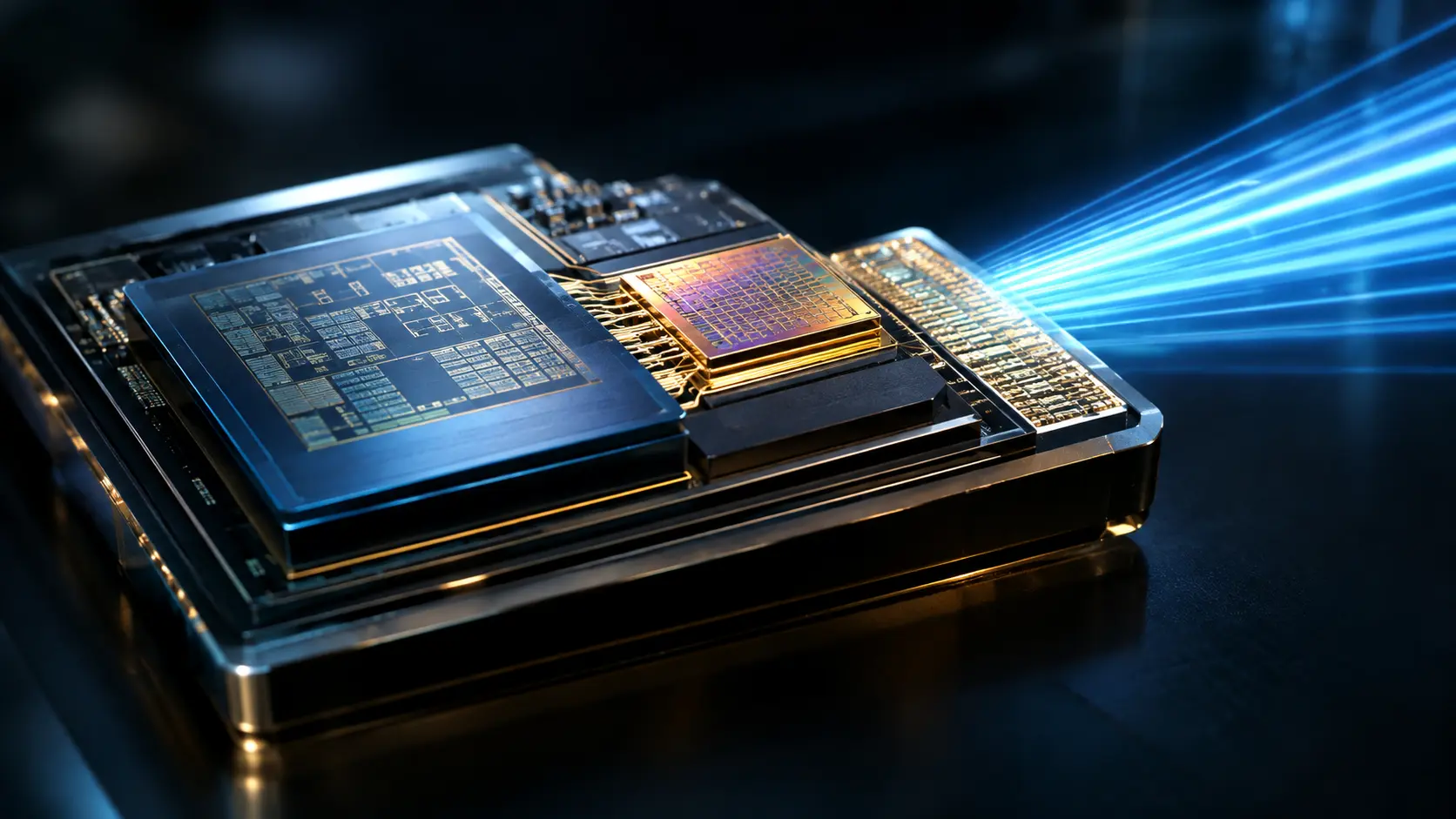

For the past fifty years, the entire digital economy has been built on a single, cheap, ubiquitous material: Silicon. Every smartphone, computer, and 5G cell tower relies on silicon CMOS chips to process and transmit data. But as the world prepares for 6G, the laws of physics are forcing a violent divorce. 6G promises to deliver data at 1 Terabit per second—fast enough to download an entire 4K movie library in one second or project real-time, uncompressed holographic video. To carry that much data, the network must broadcast at frequencies above 100 Gigahertz (the Sub-Terahertz spectrum).
Why should you care right now? Because at 100 GHz, silicon stops working. The transistors simply cannot switch fast enough, and the signal degrades into useless heat. To build the 6G network, the telecom and semiconductor industries are pivoting to an exotic, highly expensive compound: Indium Phosphide (InP). By replacing traditional silicon with InP heterojunction bipolar transistors (HBTs), engineers can blast signals through the air at frequencies previously thought impossible. This transition is triggering a massive supply chain upheaval, as defense contractors, telecom giants, and semiconductor foundries race to master the rare material that will form the physical backbone of the 2030 digital economy.
What are Sub-THz 6G Transceivers?
Sub-THz 6G transceivers are advanced radio frequency microchips designed to broadcast and receive data at frequencies between 100 GHz and 300 GHz. Because traditional silicon fails at these extreme speeds, these transceivers utilize exotic III-V semiconductor materials, specifically Indium Phosphide (InP), to achieve the ultra-fast switching and high power output required for Terabit-per-second wireless networks.
At a Glance
- Concept: Swapping standard silicon chips for exotic Indium Phosphide chips to broadcast radio waves at insanely high frequencies.
- Why it matters: You cannot achieve 6G speeds (1 Tbps) on current 5G frequencies. You have to move to the Sub-THz spectrum, and InP is the only material that can efficiently power a signal at that level.
- Who uses it: Defense/aerospace (historically), and now telecom giants (Ericsson, Nokia) partnering with advanced foundries (GlobalFoundries, TSMC) for 6G deployment.
- Biggest takeaway: InP is vastly superior to silicon for broadcasting high-frequency waves, but it is too expensive and inefficient to use for standard computer logic. Future 6G antennas will be “chiplet” hybrids: InP handling the radio waves, glued directly to a silicon chip handling the math.
In Simple Words
Think of a microchip like an engine in a car, and the radio frequency like the RPM (revolutions per minute).
A standard Silicon CMOS chip is like a reliable Honda Civic engine. It works perfectly for everyday driving (4G and 5G networks). But 6G requires the engine to spin at 300,000 RPM. If you push a Honda engine to that speed, the pistons can’t move fast enough, the engine stalls, and it melts from the friction. Silicon literally runs out of “electron mobility.”
Indium Phosphide (InP) is a Formula 1 hyper-engine built from exotic, lightweight alloys. Its internal physics allow electrons to zip through the material with almost zero friction. It can easily spin at 300,000 RPM without breaking a sweat, blasting an incredibly powerful, high-frequency signal out of the antenna. Because we are out of room on the standard radio dial, moving to these ultra-high RPMs is the only way to send more data through the air.
Why This Matters
For Telecom Execs, RF Engineers, and Semiconductor VCs, the InP transition solves the fMAX Power Wall.
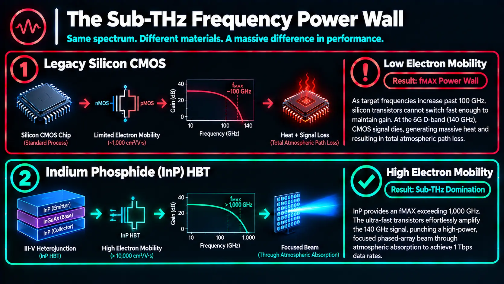
In radio frequency (RF) engineering, the most critical metric is fMAX (the maximum oscillation frequency). It dictates the absolute upper speed limit where a transistor can still provide a useful power gain. If you want to broadcast a signal at 140 GHz (the D-band targeted for 6G), you need your fMAX to be roughly three times that number to have enough power to push the signal through the air.
- Silicon CMOS hits an fMAX wall around 250 GHz to 300 GHz. At 140 GHz operation, it is choking.
- Silicon Germanium (SiGe) pushes the limit to roughly 400 GHz. It can barely handle the lower end of 6G, but it burns massive amounts of power to do so.
- Indium Phosphide (InP) routinely demonstrates an fMAX exceeding 1,000 GHz (1 THz).
Without InP, a 6G base station trying to use silicon would emit a signal so weak it couldn’t reach a smartphone 10 feet away. InP provides the raw, brute-force power amplification required to make Sub-THz wireless communication physically and economically viable.
Micro-Insight: In the semiconductor world, silicon is a digital material; it is great at 1s and 0s. InP is an analog material; it is great at pushing raw, continuous radio wave power.
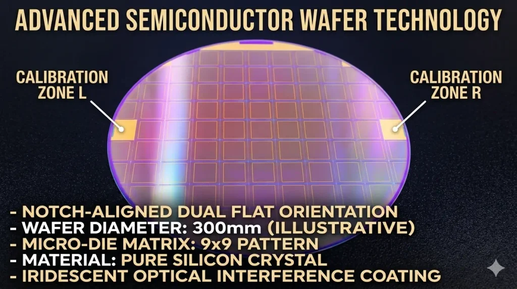
The Industrialization of III-V Compound Semiconductors
We are witnessing the industrialization of III-V Compound Semiconductors.
For decades, exotic materials from columns III and V of the periodic table (like Indium, Gallium, and Arsenic) were restricted to multi-million-dollar defense satellites and James Webb Space Telescope sensors. They were too brittle, too expensive, and too hard to manufacture for commercial use.
The demands of 6G are forcing these aerospace-grade materials down into the consumer telecom supply chain. We are moving from a monolithic world (where an entire device is printed on one piece of silicon) to a heterogeneous world—stitching different exotic elements together to survive the extreme physics of the Sub-Terahertz spectrum.
How Sub-THz 6G Transceivers Overcome Path Loss
Extracting extreme bandwidth from the Sub-THz spectrum requires navigating brutal atmospheric physics and exotic material science. Here is the first-principles breakdown of the architecture.
1. The Fundamental Problem: Path Loss and Oxygen Absorption
The higher the frequency of a radio wave, the more data it can carry, but the faster it dies in the air. Sub-THz waves (above 100 GHz) suffer from extreme “path loss.” Furthermore, water vapor and oxygen molecules in the atmosphere physically absorb these tiny waves, destroying the signal. A 6G signal fired from a traditional antenna will dissipate into heat within a few meters.
2. The Core Mechanism: InP Heterojunction Bipolar Transistors (HBTs)
To fight atmospheric absorption, the antenna must scream. It needs extreme transmit power. InP HBTs utilize a “heterojunction”—a sandwich of two different semiconductor materials (e.g., InGaAs and InP). This specific atomic structure confines electrons into a super-fast channel, allowing them to travel with incredible velocity (high mobility) while surviving high voltages (high breakdown voltage). This combination allows the InP transistor to pump massive amounts of power into the high-frequency signal without burning up.
3. Technical Depth: Massive MIMO Phased Arrays
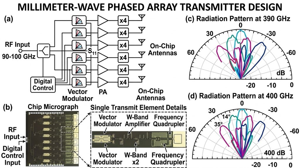
Even with InP power, a wide broadcast wave will still die quickly. 6G solves this by not broadcasting in all directions. Instead, the transceiver uses a Phased Array—a grid of hundreds of microscopic antennas. By slightly delaying the signal to certain antennas in the grid, the transceiver forces the radio waves to collide and combine, forming a hyper-focused, laser-like “pencil beam.” This beam cuts through the atmosphere directly to a user’s smartphone.
4. Technical Depth: Heterogeneous Integration (2.5D/3D Packaging)
Here is the catch: InP is amazing at shooting the radio beam, but it is terrible at doing the math to aim the beam. Silicon CMOS is required for the digital math.
Therefore, engineers use Heterogeneous Integration. They manufacture the “brain” (the digital modem) out of cheap Silicon CMOS. They manufacture the “mouth” (the power amplifier) out of exotic InP. Using advanced 2.5D or 3D packaging, they glue the tiny InP chiplet directly on top of the Silicon chip.
5. Real-World Consequences: Microscopic Insertion Loss
Because the frequency is so high, the physical wire connecting the Silicon brain to the InP mouth must be unimaginably short. If the connection is even a fraction of a millimeter too long, the 140 GHz signal will leak out as “insertion loss” before it even reaches the antenna. The manufacturing tolerance required to align these two different materials is the single hardest mechanical challenge in the 6G hardware rollout.
6G Material RF Performance Simulator
fMAX Cutoff, Atmospheric Absorption, and the Indium Phosphide Transition
Target Broadcast Frequency
140 GHz (D-Band)
Semiconductor Material
Silicon CMOS
SiGe BiCMOS
Indium Phosphide (InP)
Available Power Gain (GMAX)
+17.1 dB
fMAX Headroom (Margin)
+860 GHz
6G Link Viability
1.0 Tbps Unlocked
Sub-THz Beamforming & Atmospheric Propagation
HIGH-GAIN PENCIL BEAM
Transistor Power Gain vs. Frequency (fMAX Cutoff Spectrum)
Commercial Deployments of InP 6G Hardware
The transition to InP Sub-THz transceivers is unlocking the use cases that 5G promised but failed to deliver.
Holographic Telepresence: 6G aims to deliver true, volumetric 3D holograms in real-time. This requires streaming uncompressed spatial data at speeds approaching hundreds of gigabits per second. Traditional mmWave 5G cannot handle this payload. InP-powered D-band (140 GHz) transceivers provide the massive continuous spectrum blocks required to push volumetric video with sub-millisecond latency, making remote robotic surgery and lifelike telepresence viable.
Joint Communication and Sensing (JCAS): At Sub-THz frequencies, radio waves are so small they act like radar. 6G base stations equipped with InP transceivers will not just broadcast internet; they will simultaneously map the physical environment in high-resolution 3D. A cell tower will be able to provide 1 Tbps internet to a self-driving car while simultaneously acting as an ultra-precise radar, tracking pedestrians and obstacles around corners.
Wireless Data Center Backhaul: Laying fiber-optic cables between buildings in a dense urban environment or across a massive hyperscale data center campus is incredibly expensive and slow. InP transceivers can establish point-to-point wireless links operating at 200+ GHz, blasting fiber-optic speeds through the air. This allows cloud providers to rapidly scale server clusters without digging trenches.
Strategic Impact on the Global Foundry Monopoly
The core strategic consequence of the InP transition is the Fragmentation of the Foundry Monopoly.
For decades, Taiwan Semiconductor Manufacturing Company (TSMC) has utterly dominated the global digital economy by mastering the scaling of pure Silicon CMOS.
However, Indium Phosphide is a radically different beast. It requires different chemical etching, different thermal management, and different wafer handling (InP wafers are brittle and prone to shattering). Because of this, specialized RF foundries—like GlobalFoundries, Tower Semiconductor, and defense-centric fabs like Northrop Grumman’s internal foundries—are gaining massive strategic leverage. The telecom giants must partner with these specialized III-V foundries to build the 6G RF front-end, breaking the absolute hegemony of the pure-play silicon giants over telecommunications infrastructure.
Advantages
- Extreme Bandwidth Capacity: Unlocks the continuous blocks of spectrum available above 100 GHz, enabling true 1 Tbps data rates.
- Superior Output Power: Delivers vastly higher transmit power at Sub-THz frequencies compared to Silicon or SiGe, physically punching the signal through atmospheric absorption.
- High Electron Mobility: Electrons move through InP significantly faster than silicon, minimizing transit delays and enabling sub-millisecond network latencies.
- Miniaturization of Antennas: As frequency goes up, antenna size goes down. At 140 GHz, the antennas are microscopic, allowing massive 256-element phased arrays to be printed directly onto a chip the size of a postage stamp.
Limitations
- Astronomical Wafer Costs: A standard 300mm silicon wafer costs roughly $150 to manufacture. InP wafers are incredibly difficult to grow, max out at 150mm (6 inches), and can cost thousands of dollars per wafer.
- Thermal Density (Overheating): InP pumps out massive power from a microscopic footprint. Dissipating the extreme heat generated by a dense 6G phased array requires exotic cooling solutions, complicating smartphone integration.
- Packaging Friction: Taking a brittle InP power amplifier chiplet and co-packaging it perfectly alongside a silicon modem without losing the high-frequency signal at the solder joint is currently causing high defect rates in manufacturing.
Takeaway: InP wins the physics battle flawlessly, but it is currently losing the economics battle. The entire industry is racing to figure out how to mass-produce an aerospace-grade material at consumer-electronics prices.
Common Misconceptions
Misconception: 6G will completely replace silicon.
Reality: Silicon will still do 90% of the work. Silicon will run the core network, the digital modems, and the AI processing. InP will only be used for the “last millimeter”—the specific power amplifier that actually touches the antenna.
Misconception: 6G Sub-THz waves will go through walls.
Reality: They absolutely will not. Sub-THz waves are so small and fragile they can be blocked by a piece of paper, human skin, or heavy rain. 6G Sub-THz networks will require line-of-sight and will primarily be used for outdoor urban corridors or indoor stadiums.
Misconception: InP is a brand new discovery.
Reality: Indium Phosphide has been used for decades in fiber-optic lasers and classified military radars. What is new is the attempt to miniaturize it and make it cheap enough to put in a commercial cell tower.
What Most People Miss
The disruptive capability of The SiGe Stopgap.
When analysts discuss 6G, they often frame it as a direct jump from Silicon CMOS to InP. What they miss is the brutal pragmatism of the telecom industry.
Because InP is so difficult to package, many telecom hardware providers are fiercely trying to stretch Silicon Germanium (SiGe) BiCMOS to its absolute breaking point to cover the lower end of the 6G spectrum (e.g., 100-140 GHz). SiGe is slightly slower than InP, but it is deeply compatible with existing silicon manufacturing lines, making it vastly cheaper. The defining battle of the late 2020s will be whether SiGe can hit the minimum power requirements for early 6G, or if the industry will be forced to swallow the massive CapEx pill of moving straight to InP.
Comparison Table
| Metric | Silicon CMOS | Silicon Germanium (SiGe) | Indium Phosphide (InP) HBT |
| Primary 6G Use Case | Digital Baseband / Logic | Lower Sub-THz (100-140 GHz) | Upper Sub-THz (140-300 GHz) |
| fMAX Limit | ~300 GHz | ~400 GHz | > 1,000 GHz (1 THz) |
| Manufacturing Cost | Extremely Low | Moderate | Extremely High |
| Wafer Size Limit | 300mm (Massive scale) | 300mm | 150mm (Low scale) |
| Output Power at 140 GHz | Very Poor (Signal dies) | Adequate | Exceptional |
Future Outlook
Next 12–24 Months
The era of Heterogeneous Packaging Validation. Through 2027, the primary focus of the semiconductor industry will not be the InP material itself, but the glue. Foundries like TSMC and Intel Foundry will aggressively push 2.5D and 3D advanced packaging techniques to prove they can mount InP chiplets onto silicon interposers with acceptable yield rates. Success here is the absolute prerequisite for commercializing 6G hardware.
Next 3–5 Years
The scaling of D-Band Point-to-Point Deployments. By 2030, early 6G will not be on your smartphone. The first commercial deployment of InP Sub-THz transceivers will be in “Fixed Wireless Access” (FWA) and cell tower backhaul. Telecoms will mount small D-band (140 GHz) dishes on city rooftops, using the massive InP bandwidth to securely beam 100 Gbps fiber-optic speeds through the air between buildings, bypassing the regulatory nightmare of digging up city streets.
Next 10 Years
The Ubiquitous Sub-THz Cellular Mesh. By the mid-2030s, the economies of scale will finally drive down the cost of InP wafers. 6G Sub-THz transceivers will be miniaturized enough to integrate into premium consumer devices (AR/VR headsets and smartphones). Because Sub-THz waves cannot penetrate walls, the network architecture will shift from massive, centralized cell towers to a dense mesh of millions of microscopic InP antennas embedded in streetlights, smart windows, and indoor ceiling tiles, ensuring constant line-of-sight gigabit coverage.
Most Likely Scenario
The physical limitations of the electromagnetic spectrum dictate that 6G must move into the Sub-Terahertz regime to achieve its promised speeds. The thermodynamic and mobility limits of silicon dictate that it cannot survive there. Therefore, the transition to III-V materials like Indium Phosphide for RF power amplification is a strict mathematical certainty. While the supply chain friction and packaging costs will delay broad consumer rollout, the strategic necessity of Terabit wireless data will ultimately force the successful commercialization of the InP hybrid architecture.
Key Takeaways
- To achieve the 1 Terabit per second speeds promised by 6G, networks must broadcast at extreme Sub-THz frequencies (100 GHz to 300 GHz).
- Traditional Silicon microchips hit a “power wall” around 200 GHz. They cannot switch fast enough to push a signal through the air, rendering them useless for 6G radio transmission.
- Indium Phosphide (InP) is an exotic material that allows electrons to move incredibly fast. It can easily generate the massive power needed to broadcast Sub-THz frequencies.
- Because InP is very expensive and hard to manufacture, 6G chips will use “heterogeneous integration”—gluing a small, powerful InP radio chip directly onto a large, cheap Silicon digital “brain.”
- This transition breaks the dominance of pure-silicon foundries, empowering specialized RF foundries and defense contractors who have mastered exotic III-V materials.
Glossary
D-Band / G-Band: Specific ranges of the electromagnetic spectrum targeted for 6G. The D-band is roughly 110-170 GHz, and the G-band is 140-220 GHz.
fMAX (Maximum Oscillation Frequency): The absolute speed limit of a transistor. It is the frequency at which the transistor can no longer amplify a signal, outputting only as much power as it takes in.
Heterojunction Bipolar Transistor (HBT): A type of transistor built by layering different semiconductor materials (a heterojunction) to trap electrons in a super-fast channel, perfect for high-frequency power amplification.
Heterogeneous Integration: The advanced manufacturing technique of taking different types of microchips (made of different materials like Silicon and InP) and packaging them tightly together as if they were one single chip.
III-V Semiconductors: Materials composed of elements from columns III and V of the periodic table (like Indium and Phosphorous). They have vastly superior electrical and optical properties compared to basic Silicon (Column IV).
Massive MIMO Phased Array: An antenna composed of hundreds of microscopic individual elements that work together to electronically steer and focus a radio signal into a tight, powerful beam.
Sources
IEEE Microwave Magazine: The Race to 6G: Sub-THz Transceiver Architectures and InP HBTs
Nokia Bell Labs: D-Band and Beyond: The Physics of Sub-THz Propagation for 6G
GlobalFoundries: Heterogeneous Integration of Silicon and III-V Materials for Next-Gen RF
MIT Center for Integrated Circuits and Systems: fMAX Scaling Limits in CMOS and BiCMOS Technologies
International Telecommunication Union (ITU): IMT-2030 (6G) Vision and Spectrum Requirements