Advertisement
)
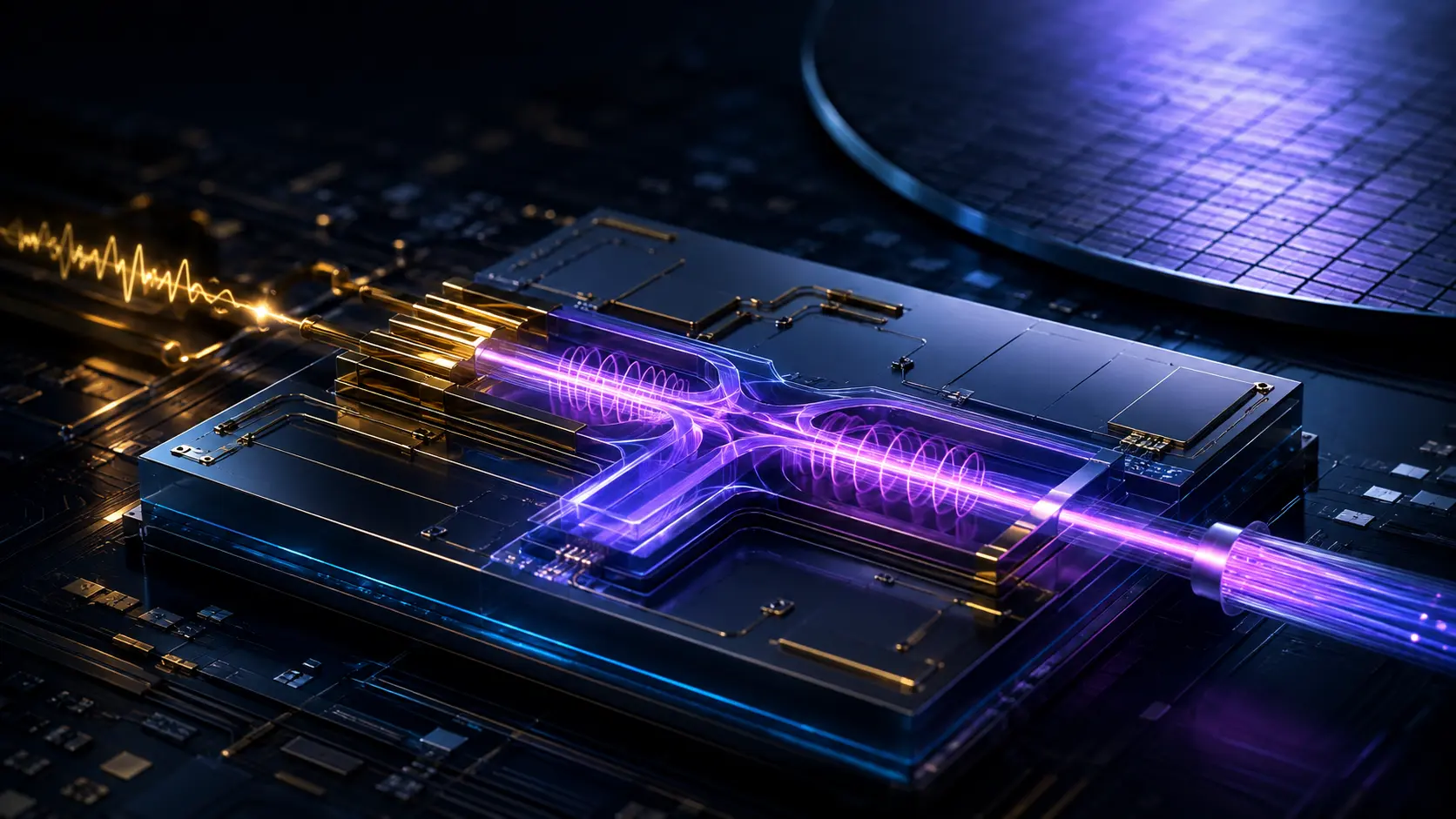

Imagine you have just built a $1 billion supercomputer packed with the fastest AI chips on Earth. Now, try to get the data out of those chips. As artificial intelligence models scale past a trillion parameters, the limiting factor isn’t the silicon processors; it is the physical wires connecting them. In modern data centers, data is translated into light and shot across fiber-optic cables using Silicon Photonics. But silicon has hit a physical wall. To transmit data fast enough to feed a modern AI cluster, silicon optical modulators burn staggering amounts of electricity and distort the signal at extreme speeds. The AI revolution is literally bottlenecked by the physics of light conversion.
Why should you care right now? Because the semiconductor industry is abandoning standard silicon to build the next generation of the internet. To shatter the “power wall,” engineers have turned to an exotic, lab-grown crystal called Thin-Film Lithium Niobate (TFLN). By harnessing the quantum physics of the “Pockels effect,” TFLN chips translate digital data into light at 220 GHz speeds while consuming a microscopic fraction of the energy.As the global supply chain rapidly transitions to mass-producing massive 200mm (8-inch) TFLN wafers, this crystalline technology is poised to replace legacy silicon photonics, rewiring the architecture of hyperscale data centers and unlocking the multi-terabit future of artificial intelligence.
What is Thin-Film Lithium Niobate (TFLN)?
Thin-Film Lithium Niobate (TFLN) is an advanced electro-optic material used to manufacture high-speed optical modulators for fiber-optic networks. By leveraging a high Pockels coefficient, TFLN chips convert electrical data into laser light signals at sub-terahertz speeds with ultra-low power consumption, fundamentally outperforming legacy silicon photonics in AI data centers.
At a Glance
- Concept: A crystalline microchip that turns electrical data (1s and 0s) into flashing laser light faster and far more efficiently than standard silicon.
- Why it matters:AI clusters require 1.6 Terabit-per-second (Tbps) and 3.2 Tbps optical connections. Silicon photonics burns too much power at these speeds. TFLN solves the “power wall,” drastically reducing the electricity needed to move data.
- Who uses it: Hyperscale cloud providers, telecommunications giants (6G networks), and advanced optical transceiver manufacturers.
- Biggest takeaway: TFLN utilizes the “Pockels effect.” Applying a tiny electrical voltage to the crystal physically alters the speed of light traveling through it instantly, without generating excess heat or absorbing the light.
In Simple Words
Imagine you need to send Morse code using a flashlight.
If you use a Silicon Photonics flashlight, the switch is heavy and sticky. You can flick it on and off fast, but if you try to do it millions of times a second, your thumb gets exhausted (high power consumption), the switch heats up, and the light starts to flicker unpredictably.
A Thin-Film Lithium Niobate (TFLN) flashlight doesn’t use a mechanical switch. It uses a magical crystal lens. Instead of physically blocking the light, you apply a tiny, almost imperceptible electrical zap to the crystal. The zap instantly alters how the light passes through the crystal, dimming it or brightening it perfectly. Because you aren’t fighting mechanical friction or heavy electrical resistance, you can “flick” the light on and off hundreds of billions of times a second without breaking a sweat, sending massive amounts of data with barely any electricity.
Why This Matters
For Cloud Architects, Hardware Engineers, and Tech Investors, TFLN is the ultimate weapon against the Data Center Thermal Budget.
An AI data center only has a finite amount of electricity coming from the local power grid. If the optical transceivers (the plugins that connect the servers) consume 30 Watts of power each just to move data, thousands of transceivers will consume megawatts of the facility’s total power budget—leaving less electricity available for the actual GPUs doing the math. By transitioning from silicon photonics to TFLN, the energy required to modulate the light collapses to as low as 0.69 fJ/bit. This fractional energy footprint frees up massive amounts of electricity, allowing cloud architects to pack vastly more AI compute into the exact same physical server rack.
The Evolution of Lithium Niobate in Telecom
Lithium Niobate (LiNbO₃) is not a new material. “Bulk” lithium niobate has been the undisputed gold standard for long-haul submarine telecom cables since the 1990s because of its flawless signal fidelity.
However, bulk LN modulators were the size of a cigar—far too large and expensive to fit inside a modern, high-density AI server rack. Silicon photonics won the 2010s because silicon could be miniaturized and printed cheaply using standard computer chip factories. The monumental breakthrough of the 2020s is the “Thin-Film” architecture. By slicing the crystal into a microscopic layer (300 to 700 nanometers thick) and bonding it onto an insulator (LNOI), scientists successfully miniaturized the gold standard of telecommunications down to the nanoscale.
How TFLN Optical Modulators and the Pockels Effect Work
Bypassing the speed of silicon requires exploiting the quantum electro-optic properties of anisotropic crystals. Here is the first-principles breakdown of the architecture.
1. The Fundamental Problem: Silicon’s Free-Carrier Effect
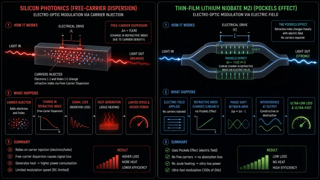
Silicon does not possess a natural electro-optic effect. To modulate light in a silicon chip, engineers use the “free-carrier dispersion effect”—they physically inject or remove electrons into the optical path to change how light travels. Moving physical electrons takes time, causes resistance (heat), and actually absorbs some of the light photons. At speeds past 100 GHz, this process hits a hard physical wall of inefficiency.
2. The Core Mechanism: The Pockels Effect
TFLN utilizes the linear electro-optic Pockels effect (r₃₃ ≈ 31 pm/V). When an electric field (voltage) is applied to the lithium niobate crystal, it distorts the electron clouds surrounding the atoms. This distortion instantly changes the refractive index of the crystal, altering the speed of the light passing through it. Crucially, no actual electrons are injected into the optical path, meaning zero light is absorbed and the reaction happens at the absolute speed of sub-atomic physics.
3. Technical Depth: Mach-Zehnder Interferometers (MZI)
TFLN modulators typically use a Mach-Zehnder Interferometer structure. The incoming laser light is split into two parallel TFLN waveguides. A data signal (voltage) is applied to one or both arms via electrodes. The Pockels effect speeds up the light in one arm and slows it down in the other. When the two paths recombine, the light waves are “out of phase” and cancel each other out (destructive interference). By rapidly turning the voltage on and off, the chip turns a steady laser beam into a blinking stream of 1s and 0s.
4. Bypassing the Driver Amplifier: Sub-Volt Vπ
The voltage required to push the light waves completely out of phase is known as the half-wave voltage (Vπ). In bulky legacy devices, Vπ was high (5V+), requiring power-hungry driver amplifiers to boost the signal.
Because TFLN confines the light into a microscopic 300-nm trench, the gold electrodes can be placed incredibly close to the light beam. This proximity generates an intensely strong electric field, dropping the Vπ to sub-2V or even sub-1V. At this low voltage, the main CMOS computer chip can drive the optical modulator directly, completely eliminating the need for an external amplifier and saving massive amounts of power.
5. Real-World Consequences: 220 GHz at 0.69 fJ/bit
Because it relies on the frictionless Pockels effect and sub-volt driving requirements, a modern TFLN modulator can operate at extrapolated bandwidths of 220 GHz—the absolute foundation necessary for 1.6 Tbps and 3.2 Tbps single-wavelength transmission.This extreme speed is achieved with transformative energy efficiency, drawing as little as 0.69 femtojoules per bit (0.69 fJ/bit), permanently shattering the silicon power wall.
Commercial Applications: Transceivers and Co-Packaged Optics (CPO)
TFLN is aggressively shifting from a laboratory curiosity into the foundational hardware of the global telecommunications supply chain.
1.6T and 3.2T Optical Transceivers: The immediate commercial application for TFLN is inside the pluggable transceivers that connect massive AI GPU clusters (like NVIDIA NVLink switches). As AI models demand higher throughput, networks are upgrading to 1.6 Tbps standards. TFLN allows hardware manufacturers to hit these astronomical speeds without melting the transceiver casing, ensuring stable, low-latency data flow between thousands of parallel GPUs.
Co-Packaged Optics (CPO): The ultimate goal of data center architecture is Co-Packaged Optics, where the optical lasers and modulators are moved off the pluggable cables and packaged directly onto the same silicon substrate as the main switch ASIC. TFLN’s microscopic footprint and sub-1V drive requirements make it the ideal material for CPO integration, allowing the main processor to talk directly to the fiber-optic network natively.
Quantum Key Distribution (QKD): Quantum networking relies on entangled photon pairs. Lithium Niobate has a massive second-order nonlinear coefficient (d₃₃ ≈ -27 pm/V, μTP), making it the perfect material for “spontaneous parametric down-conversion”—the process of taking one high-energy photon and splitting it into two perfectly entangled lower-energy photons. TFLN chips are becoming the standard engines for secure, unhackable quantum communication grids.
Economic & Strategic Impact
The core strategic inflection point for TFLN is the Transition to 200mm Wafer Scale.
For years, the primary criticism of Lithium Niobate was that it was a “cottage industry.” Crystals were grown slowly and sliced into small 4-inch or 6-inch wafers, making the chips too expensive for mass-market data centers.
By 2026, the supply chain executed a monumental leap to 200mm (8-inch) TFLN wafer manufacturing. This transition allows TFLN to be processed using the exact same robotic foundry tools used for legacy silicon chips. This economies-of-scale breakthrough drastically crashes the “per-die” cost of a TFLN modulator. The ability to mass-produce TFLN at silicon-like prices effectively removes the last remaining barrier to entry, threatening to completely usurp the established silicon photonics monopolies currently dominating the data center market.
Advantages
- Ultra-High Bandwidth:Routinely exceeds 100 GHz, with leading-edge designs achieving 220 GHz, mathematically supporting multi-terabit data streams.
- Zero-Loss Linear Modulation:The Pockels effect preserves absolute signal fidelity across a wide dynamic range, avoiding the two-photon absorption and signal distortion inherent in silicon.
- Extreme Energy Efficiency:Sub-2V drive requirements allow the chip to be driven directly by CMOS electronics, eliminating hot, expensive amplifier chips and pushing energy consumption below 1 fJ/bit.
- Broad Transparency Window:TFLN is transparent to light across a massive spectrum (from 350 nm visible light all the way to 5 µm mid-infrared), making it vastly more versatile than silicon.
Limitations
- Etching Difficulty: Silicon is chemically easy to etch into perfect microscopic shapes. Lithium Niobate is notoriously tough and chemically inert. Etching TFLN waveguides often leaves rough, slanted sidewalls, which can scatter light and cause optical loss if not perfectly polished.
- Cost vs. Silicon:Despite the 200mm wafer transition, the raw TFLN-on-insulator (LNOI) blank wafers are still significantly more expensive to manufacture than standard silicon-on-insulator (SOI) wafers.
- Lack of Native Lasers or Detectors: TFLN is brilliant at modulating light, but it cannot generate or detect light. To build a complete optical system, manufacturers must still bond Indium Phosphide (InP) lasers and Germanium detectors onto the TFLN chip, adding packaging complexity.
Common Misconceptions
Misconception: TFLN will replace Silicon entirely in computers.
Reality: TFLN only replaces Silicon Photonics (the parts that move light). The actual “brain” doing the math (the CPU or GPU) will remain standard CMOS silicon for the foreseeable future.
Misconception: The Pockels effect is a new discovery.
Reality: The Pockels effect was discovered in 1906, and bulk LN modulators have been used since the 1990s. The true innovation is the “Thin-Film” packaging—figuring out how to slice the crystal to 300 nanometers and bond it to a microchip.
Misconception: TFLN consumes zero power.
Reality: While the Pockels effect itself consumes practically zero power, the electrical wires pushing the microwave voltage down the chip still encounter electrical resistance, generating minor thermal loss.
What Most People Miss
The disruptive intelligence value of Heterogeneous Integration (Micro-Transfer Printing).
The fierce debate in the industry is often framed as “Silicon vs. TFLN.” What most analysts miss is that the winning architecture isn’t a competition; it is a fusion.
Because silicon is excellent for routing light and cheap to manufacture, but terrible at modulating it, engineers are aggressively pursuing Heterogeneous Integration.Using techniques like Micro-Transfer Printing (μTP), automated robots literally pick up microscopic “chiplets” of TFLN and paste them directly on top of a standard 200mm Silicon Photonics wafer. This allows the cheap silicon to handle all the basic plumbing, while the expensive TFLN handles the heavy lifting of ultra-fast modulation. This “best of both worlds” approach bypasses the need to etch TFLN perfectly and leverages billions of dollars of existing silicon foundry infrastructure.
Comparison Table
| Feature | Legacy Bulk Lithium Niobate | Silicon Photonics (SiPh) | Thin-Film Lithium Niobate (TFLN) |
| Modulation Mechanism | Pockels Effect | Free-Carrier Dispersion | Pockels Effect |
| Max Bandwidth | ~40 GHz | ~100 GHz (Starts distorting) | > 200 GHz (Ultra-linear) |
| Drive Voltage (Vπ) | High (5V+) | Moderate (2V – 3V) | Very Low (< 2V, sub-1V) |
| Device Size | Massive (Centimeters) | Microscopic | Microscopic |
| Energy per Bit | Very High | Moderate | Ultra-Low (0.69 fJ/bit) |
| Primary Use Case | Legacy Submarine Cables | 400G / 800G Data Centers | 1.6T+ AI Interconnects & 6G |
Case Study
Situation: The exponential scaling of generative AI workloads dictated that next-generation GPU clusters required 1.6 Tbps to 3.2 Tbps optical interconnects to prevent massive data bottlenecks. Traditional silicon photonics faced severe free-carrier absorption limits at >100 GHz bandwidths, requiring excessive thermal design power (TDP) just to drive the optical modulators, threatening to melt the server racks.
Challenge: Develop a highly scalable, ultra-fast electro-optic modulator capable of supporting single-wavelength 1.6 Tbps transmission without exceeding the strict energy constraints of a hyperscale data center.
Solution (The 200mm LNOI Wafer Transition): Global photonics foundries and research hubs abandoned bulk LN and transitioned to Thin-Film Lithium Niobate on Insulator (LNOI).By leveraging the 31 pm/V Pockels coefficient of TFLN and mastering the dry-etching of monolithic ridge waveguides on scaled 200mm (8-inch) wafers, engineers achieved perfect velocity matching between microwave data signals and optical light waves.
Outcome: The resulting TFLN modulators demonstrated extrapolated bandwidths of 220 GHz, operating with sub-2V drive voltages.Because the modulators could be driven natively by CMOS logic without heavy amplification, the energy consumption of the optical link collapsed to 0.69 fJ/bit.
Lessons Learned: The breakthrough validated that material science, not just circuit design, is the ultimate key to breaking the memory and networking walls of modern computing. By shifting to a 200mm scalable wafer process, the industry proved that the superior quantum properties of Lithium Niobate could finally be democratized for mass-market AI deployment.
Future Outlook
Next 12–24 Months
The era of 1.6T Pluggable Dominance. In the immediate term, TFLN will completely consume the premium tier of the optical transceiver market. As NVIDIA, AMD, and Broadcom roll out their next-generation AI switching fabrics, hardware vendors will rapidly deploy 800G and 1.6T pluggable modules powered exclusively by TFLN modulators.Silicon photonics will be relegated to cost-sensitive, short-reach, lower-bandwidth enterprise applications, while TFLN becomes the mandatory standard for any hyperscale environment constrained by power and thermal limits.
Next 3–5 Years
The scaling of Monolithic LiDAR and 6G Terahertz. As TFLN foundries mature, the technology will expand beyond data centers. TFLN’s ability to manipulate the phase of light instantly and without loss makes it the ultimate platform for Optical Phased Arrays (OPAs)—the solid-state laser steering engines required for next-generation, high-resolution LiDAR in autonomous vehicles.Concurrently, TFLN will be integrated into 6G telecommunications infrastructure, serving as the bridge to seamlessly convert sub-terahertz radio frequencies into optical fiber signals with ultra-low phase noise.
Next 10 Years
The Heterogeneous Quantum Computing Backbone. By the mid-2030s, pure optical computing and quantum networking will leave the laboratory. TFLN’s immense second-order nonlinearity makes it unparalleled for generating squeezed light and entangled photon pairs.Through advanced die-to-wafer bonding and micro-transfer printing, TFLN will be permanently hybridized with silicon, creating massive, wafer-scale quantum photonic integrated circuits (PICs). These monolithic chips will process, entangle, and route quantum information at room temperature, forming the physical hardware layer of the global quantum internet.
Most Likely Scenario
Thin-Film Lithium Niobate guarantees the continuous scaling of global data infrastructure. By executing the exact same miniaturization playbook that made silicon successful, but applying it to a vastly superior crystalline material, the photonics industry has secured its runway for the next two decades. TFLN is not a stepping stone; it is the definitive, physically optimal architecture for transforming electricity into light.
Key Takeaways
- To connect massive AI supercomputers, data is turned into light using optical modulators. Silicon photonics, the current standard, burns too much power and distorts signals at the extreme speeds AI requires.
- Thin-Film Lithium Niobate (TFLN) is a synthetic crystal microchip that solves this. It translates data into light at sub-terahertz (220 GHz) speeds with virtually zero signal loss.
- It works via the “Pockels effect.” Applying a tiny voltage instantly changes the speed of light through the crystal without using heavy mechanical switches or injecting heat-generating electrons.
- Because the chip requires very little voltage (Vπ < 2V), it bypasses the need for power-hungry amplifier chips, plunging its energy consumption to an incredibly efficient 0.69 fJ/bit.
- The technology is finally leaving the lab because the industry has figured out how to mass-produce it on standard 200mm (8-inch) semiconductor wafers, making it cheap enough for mass data center deployment.
- Rather than fully replacing silicon, future chips will likely “glue” microscopic pieces of TFLN directly on top of cheap silicon routing boards to get the best of both worlds.
Glossary
Co-Packaged Optics (CPO): A futuristic hardware design where the optical lasers and modulators are packed directly onto the same chip as the main computer processor, rather than plugging in external cables.
Free-Carrier Dispersion: The physical method silicon uses to modulate light by injecting electrons into the light’s path. It is slow, causes signal loss, and creates heat.
Half-Wave Voltage (Vπ): The exact amount of electrical voltage required to flip the phase of a light wave to turn the optical signal on or off. A lower Vπ means a much more power-efficient chip.
Mach-Zehnder Interferometer (MZI): A structure that splits a laser beam into two paths, slows one path down, and recombines them. If they recombine out of phase, they cancel each other out, creating the “0” in digital data.
Micro-Transfer Printing (μTP): An advanced manufacturing technique where robotic stamps pick up microscopic pieces of TFLN and bond them perfectly onto a standard silicon wafer.
Pockels Effect: A linear electro-optic effect where applying an electric field physically alters a crystal’s refractive index instantly, without absorbing light or generating heat.
Sources
arXiv: Ultra-High-Efficiency Dual-Band Thin-Film Lithium Niobate Modulator Incorporating Low-k Underfill with 220 GHz Extrapolated Bandwidth
Photonics Media: The Return of Lithium Niobate — From Bulk Modulators to Integrated Photonics
Liobate: What Is Thin Film Lithium Niobate (TFLN)? [2026 Guide]
Liobate: TFLN Capabilities and Pockels Coefficient Specifications
ResearchGate: Micro-Transfer Printing of Lithium Niobate on 200 mm Silicon Photonics
Emergent Mind: Heterogeneous Integration of Silicon Photonics and Thin-Film Lithium Niobate (TFLN)