Advertisement
)


AT A GLANCE
- Concept: Aspect Ratio: The extreme mathematical depth of the vertical tunnel compared to its microscopic width.
- Concept: Electrodeposition: Using electrical current inside a chemical bath to grow solid copper atoms from a liquid.
- Concept: Bottom-Up Fill: Forcing the copper to fill the microscopic hole strictly from the floor upward.
- Concept: Suppressor Additives: Organic chemicals that intentionally block copper from attaching to the top edges of the hole.
HOW A THROUGH-SILICON VIA WORKS
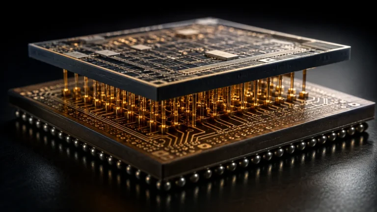
Modern silicon transistors are reaching their absolute physical limits on a flat, two-dimensional plane. To continue scaling computing performance, engineers now stack chips vertically into 3D architectures. This requires drilling thousands of microscopic holes entirely through the silicon wafers to connect the bottom chip to the top chip.
Once machines etch these deep vertical tunnels, foundries must fill them with highly conductive metal. If you submerge a silicon wafer into a standard copper electroplating bath, the metal deposits uniformly across all exposed surfaces. Because the tunnel is incredibly narrow and deep, the copper grows on the sidewalls and quickly bridges across the top opening.
This bridging creates a physical pinch-off. It seals the top of the tunnel before the bottom finishes filling, trapping a permanent, microscopic pocket of air inside the copper wire. These internal voids act as massive electrical resistors, disrupting data transmission and generating extreme localized heat.
To solve this void formation, chemical engineers heavily manipulate the electrodeposition fluid. They introduce specialized organic molecules into the liquid bath, categorizing them as suppressors, accelerators, and levelers. Suppressors are large polymers that physically gather at the top rim of the via, blocking the electrical current and preventing copper from depositing there.
Simultaneously, smaller accelerator molecules sink deep into the bottom of the via. These molecules attract the copper ions. When the electrical current activates, the metal grows rapidly from the floor of the via upward, while the top remains wide open, completely eliminating the possibility of a trapped void.
WHY IT MATTERS NOW
Generative artificial intelligence models possess an insatiable appetite for memory bandwidth. Graphics processing units (GPUs) calculate math much faster than standard memory chips can feed them data, creating a massive infrastructural bottleneck. High-Bandwidth Memory (HBM) solves this by stacking memory directly adjacent to the processor, but HBM relies entirely on flawless Through-Silicon Vias.
A single HBM stack utilizes tens of thousands of these vertical copper pillars. If even one via in a stack contains a micro-void, the electrical resistance spikes and the entire multi-thousand-dollar component fails quality control. The chemical precision of the electrodeposition bath directly dictates the physical yield and profit margins of global AI hardware manufacturers.
This exact manufacturing step dictates the balance of power in the semiconductor foundry business. Companies like TSMC and Samsung fiercely guard the proprietary recipes of their chemical plating baths. The ability to execute perfect, high-aspect-ratio bottom-up fills allows these foundries to offer the advanced chiplet packaging that companies like Nvidia and AMD require.
By mastering this vertical interconnect geometry, the industry mathematically bypasses the traditional limitations of single-chip manufacturing. Foundries can now physically separate the logic processor from the memory array, manufacture them on completely different silicon nodes, and stitch them together vertically with perfect electrical efficiency.
WHAT MOST PEOPLE MISS
Hardware commentators frequently treat 3D advanced packaging as a mechanical assembly challenge involving stacking blocks. They entirely miss that TSV creation is fundamentally a complex fluid dynamics and organic chemistry problem.
The electrical current used during the plating process constantly changes the localized concentration of the organic additives in real time. Managing the transient depletion of these specific molecules requires extreme, continuous telemetry. The silicon foundry must operate as a highly volatile chemical control loop, where a variance of parts-per-billion in the suppressor fluid ruins the entire batch of silicon.
THE TRAJECTORY
Next 12–36 Months: Hybrid bonding will aggressively replace traditional microbumps, requiring much tighter TSV pitch and deeper aspect ratios. Foundries will deploy advanced multi-step electrodeposition currents to precisely manage the chemical gradients inside increasingly narrow, sub-micron trenches.
Next Five Years: The structural transition from copper to alternative metals like ruthenium or molybdenum. Copper requires thick physical barrier layers to prevent it from chemically poisoning the surrounding silicon. As vias shrink geometrically, these barrier layers consume too much physical volume, forcing the industry toward metals that deposit directly onto the dielectric walls.
Next Ten Years: The realization of monolithic 3D integration. The physical dimensions of vertical interconnects will shrink so drastically that foundries will etch and fill them simultaneously alongside the transistor gates themselves. This will permanently erase the historical boundary between chip fabrication and advanced packaging.
What Could Go Wrong: Severe electromigration failure. As vias become narrower and data demands increase, the physical momentum of electrons passing through the interconnect increases drastically. This electron wind slowly pushes the individual copper atoms out of place, eventually creating a void post-manufacturing and physically severing the connection entirely.
Most Likely Outcome: The absolute mastery of bottom-up electrodeposition will remain the hard physical limit of global computing architecture. Advanced chemical fluid management provides the only viable mechanism to sustain the terabyte-per-second memory bandwidths required by the next decade of artificial intelligence.
KEY TERMS
- Through-Silicon Via (TSV): A microscopic vertical electrical connection passing completely through a silicon die to connect stacked layers.
- High-Bandwidth Memory (HBM): A 3D-stacked memory architecture that utilizes thousands of vertical vias to achieve extreme data transfer rates.
- Electrodeposition: A manufacturing process utilizing electrical current to reduce dissolved metal ions, forming a solid, uniform metal coating.
- Aspect Ratio: The exact mathematical relationship between the vertical depth of an etched hole and its horizontal diameter.
- Suppressor Molecule: A specialized organic chemical additive designed to physically block metal deposition at the top edge of a microscopic trench.
SOURCES
- Applied Materials — Advanced Packaging and TSV Metallization Dynamics
- Institute of Electrical and Electronics Engineers (IEEE) — Bottom-Up Copper Electrodeposition for High Aspect Ratio TSVs
- TSMC Open Innovation Platform — 3DFabric Architecture and Advanced Copper Electroplating
- Journal of The Electrochemical Society — The Role of Organic Additives in Defect-Free TSV Filling