Advertisement
)
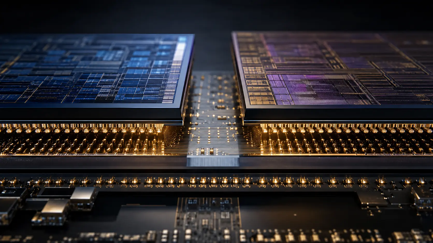

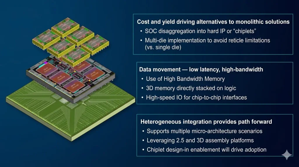
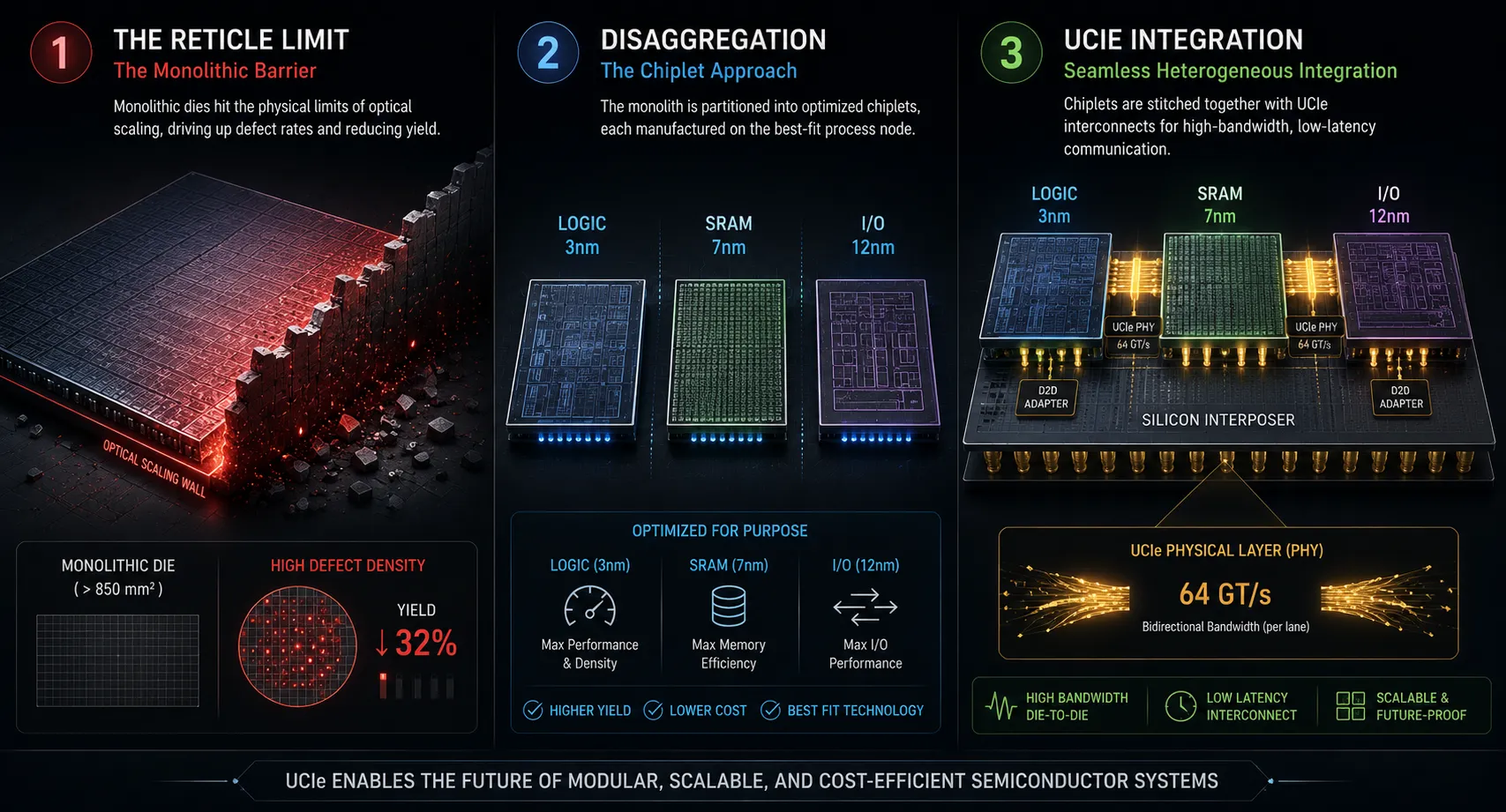
The semiconductor industry has officially crashed into a physical wall. For fifty years, chipmakers simply crammed more transistors onto a single, flat piece of silicon to make computers faster. Today, building a massive artificial intelligence processor as a single, “monolithic” piece of silicon is mathematically suicidal. The machines that print microchips have a strict optical boundary called the “reticle limit.” You cannot print a chip larger than a postage stamp. If a speck of dust lands on that massive chip during manufacturing, the entire multi-thousand-dollar piece of silicon is thrown in the trash. The math no longer works.
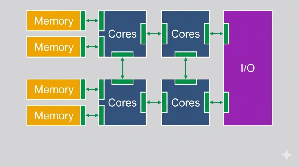
Why should you care right now? Because the fiercest rivals in human history—Intel, TSMC, and Samsung—have called a ceasefire to fix the math. Instead of building one giant chip, they are building tiny, perfect “chiplets” and stitching them together like Lego bricks. To ensure an Intel Lego brick can snap perfectly onto a TSMC Lego brick, the industry just finalized the Universal Chiplet Interconnect Express (UCIe) standard. This standard governs exactly how these microscopic blocks talk to each other at the speed of light. It is transforming the semiconductor supply chain from a closed-door monopoly into an open, interchangeable marketplace, paving the way for 3D supercomputers.
What is Universal Chiplet Interconnect Express (UCIe)?
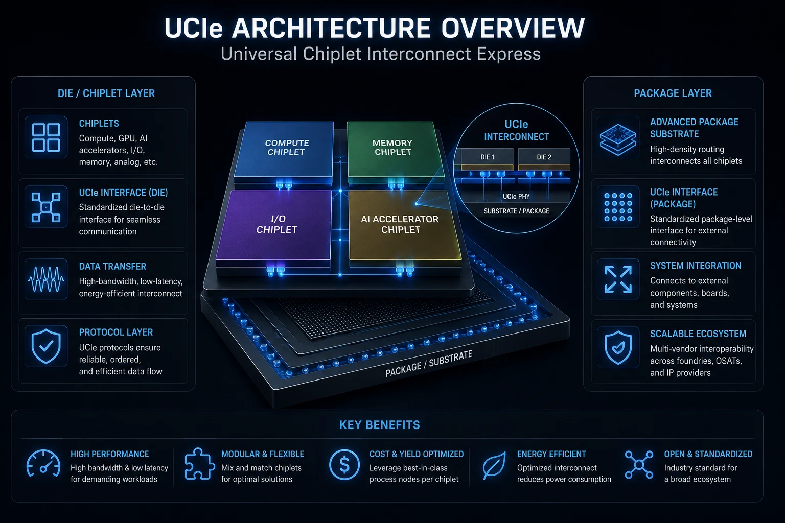
Universal Chiplet Interconnect Express (UCIe) is an open industry specification that defines the physical, electrical, and protocol standards for connecting multiple silicon chiplets within a single package. It enables heterogeneous integration, allowing manufacturers to seamlessly combine specialized chiplets fabricated by different foundries on different manufacturing nodes into one cohesive, high-performance system.
At a Glance
- Concept: The “USB port” for the inside of a microchip. A universal plug that lets tiny pieces of silicon talk to each other.
- Why it matters: It lets companies build processors larger than what physics normally allows by combining small, cheap parts instead of trying to manufacture one massive, expensive part.
- Who uses it: Vanguard semiconductor designers (AMD, Nvidia, Intel) and major foundries (TSMC, Samsung) building the next generation of AI and supercomputing hardware.
- Biggest takeaway: A company doesn’t need to be a multi-billion-dollar giant to build an AI chip anymore. A startup can build one highly specialized chiplet and plug it directly into a standard CPU using UCIe.
In Simple Words
Imagine you want to build the ultimate, massive mansion.
Historically (Monolithic Design), you had to pour a single, giant foundation and build the entire mansion in one go. If you made a single mistake in the plumbing in the guest bathroom, the city forced you to bulldoze the entire mansion and start over. Because the mansion is so big, mistakes happen constantly, making it insanely expensive.
Today (Chiplet Design), you build the mansion in a factory using small, perfect, modular rooms. You build the kitchen, the living room, and the bedroom separately. If the kitchen has a flaw, you just throw away the kitchen; you don’t ruin the rest of the house.
UCIe is the universal blueprint for the doorways connecting these modular rooms. Because of UCIe, you can buy the kitchen from Intel, the living room from TSMC, and the bedroom from Samsung. When you push the rooms together, the doors line up perfectly, the plumbing connects instantly, and the electricity flows flawlessly.
Why This Matters
For Chip Architects, Hardware VCs, and Semiconductor Engineers, UCIe solves the Heterogeneous Integration Dilemma.
Different parts of a computer require different manufacturing processes. An advanced logic core (the brain) benefits massively from being printed on an expensive 3-nanometer (3nm) node. However, the I/O controllers (the parts that talk to the outside world) do not scale well. Printing I/O on a 3nm node is a catastrophic waste of money; it works perfectly fine on an older, cheaper 12nm node.
Before UCIe, if you designed a chip, the entire chip had to be printed on the same node. UCIe allows engineers to “disaggregate” the System-on-Chip (SoC). They can print the brain on expensive 3nm silicon at TSMC, print the I/O on cheap 12nm silicon at GlobalFoundries, and stitch them together on a single package. This drastically lowers the total portfolio cost and slashes the time-to-market for new AI hardware.
The Evolution of UCIe 1.0 to 3.0 Standards
The evolution of the UCIe standard has been relentlessly aggressive to keep pace with the demands of artificial intelligence.
When UCIe 1.0 launched in 2022, it focused purely on 2D and 2.5D packaging (where chiplets sit side-by-side on an interposer). But side-by-side takes up too much space. The physical distance the data must travel drains battery power and introduces latency.
By August 2024, the consortium released UCIe 2.0, taking the standard into the vertical dimension (3D packaging). It optimized the rules for “hybrid bonding,” allowing chiplets to be stacked directly on top of each other with microscopic bump pitches down to 1 micron.In 2025/2026, the rollout of UCIe 3.0 doubled the data rate to an astonishing 64 GigaTransfers per second (GT/s), providing the ultra-dense bandwidth required for massive AI training clusters while maintaining complete backward compatibility.
How Universal Chiplet Interconnect Express Works
Stitching two microscopic pieces of glass together so they can share terabytes of data per second without melting requires a rigid, multi-layered architecture. Here is the first-principles breakdown.
1. The Fundamental Problem: Proprietary Babel
When a monolithic chip is sliced into pieces, those pieces must send data back and forth. If AMD created a chiplet, its “wires” were spaced exactly 45 microns apart and used a specific voltage. If an engineer tried to connect it to an Intel chiplet with wires spaced 55 microns apart, the data crashed.
2. The Core Mechanism: The UCIe Layered Architecture
UCIe acts as a universal translator by enforcing a strict, three-layer stack across the die-to-die (D2D) gap:
- The Physical Layer (PHY): The literal electrical and mechanical connection. It defines the exact spacing of the micro-bumps, the electrical voltages, the clock signaling, and how the data is physically blasted across the gap.
- The Die-to-Die (D2D) Adapter: The link management layer. It takes the chaotic electrical signals from the PHY and ensures they are reliable. It adds error-checking (CRC) and retry mechanisms. If a data packet gets corrupted crossing the gap, the Adapter catches it and asks for a resend.
- The Protocol Layer: The top layer. It takes the data from the Adapter and formats it into standardized software languages that the rest of the computer understands, specifically utilizing mature standards like PCI Express (PCIe) and Compute Express Link (CXL).
3. Technical Depth: Standard vs. Advanced Packaging
Not all chiplets are created equal. UCIe defines two distinct physical tracks:
- Standard Packaging: Designed for cheaper, organic substrates. The wires between chiplets are longer and less dense. It is highly cost-effective but uses more power.
- Advanced Packaging: Designed for silicon interposers or embedded multi-die interconnect bridges (EMIB). The wires are microscopically close together (high density). It offers massive bandwidth and extreme energy efficiency, but costs vastly more to manufacture.
4. Technical Depth: Lane Reversal and Repair
Silicon manufacturing is imperfect. If a single microscopic wire between two chiplets breaks during packaging, the whole multi-thousand-dollar unit would traditionally fail. The UCIe PHY layer mandates Lane Repair. It includes redundant “spare” wires. If the system detects a broken lane during boot-up, the D2D adapter automatically reroutes the data through the spare lane in real-time. It also supports Lane Reversal, allowing chiplets to be physically rotated or mirrored on the package without breaking the connection geometry.
Chiplet vs Monolithic Yield Economics
Simulating defect probability across 300mm silicon wafers
400 mm²
100 mm²
800 mm² (EUV Limit)
0.10 /cm²
Clean (0.05)
High Defect (0.50)
Manufacturing Yield
0.0%
0 Good / 0 Gross Dies
Cost Per Good System
$0
Includes baseline $15k Wafer Cost
…
Real-World Applications
The standardization of D2D interconnects is triggering a tectonic shift in how hyperscalers and automotive giants source their silicon.
Hyperscale AI Clusters: Training massive frontier models requires combining immense amounts of High Bandwidth Memory (HBM) with logic cores. Because UCIe 3.0 supports continuous transmission protocols and ultra-low latency, hyperscalers like Google and AWS can design custom AI accelerators (ASICs) that seamlessly integrate third-party HBM stacks using 3D packaging, completely removing the memory bottleneck that chokes AI data centers.
Automotive and Aerospace Resilience: Cars and fighter jets operate in extreme thermal environments where microchips degrade over time. The UCIe 2.0 and 3.0 specs introduce the UCIe DFx Architecture (UDA). This embeds a standardized management fabric directly into the chiplets for telemetry, testing, and debugging. If a specific memory chiplet inside a self-driving car’s processor starts failing, the UDA pinpoints the exact point of failure within the 3D package, allowing for predictive maintenance before a catastrophic failure occurs.
The “Chiplet Marketplace” for Startups: Historically, an AI hardware startup had to design everything—the PCIe lanes, the memory controllers, and the AI math cores—costing over $100 million in R&D. UCIe creates an “Open Chiplet Ecosystem.” The startup now only designs their proprietary AI math chiplet. They buy pre-made, validated I/O and memory chiplets from a catalog, snap them together using UCIe, and go to market for a fraction of the cost, massively lowering the barrier to entry for silicon innovation.
Economic & Strategic Impact
The core strategic consequence of UCIe is the Commoditization of Silicon Interfaces.
By standardizing the edges of the chip, the intellectual property (IP) value shifts strictly to the core computational logic. Foundries (TSMC, Samsung) and electronic design automation (EDA) companies (Synopsys, Cadence) are releasing “silicon-proven” UCIe IP blocks. If a company wants to use UCIe, they don’t invent it; they just license the pre-verified code from Synopsys and drop it onto their chip.
This commoditization threatens the walled gardens of legacy giants. If Apple, Nvidia, or Intel can no longer lock a customer into a proprietary ecosystem based on physical hardware connectors, they are forced to compete purely on the speed and efficiency of their math cores. It breaks the monolithic hardware monopoly and opens the door for hyper-customized, multi-vendor “franken-chips” tailored for specific enterprise workloads.
Advantages
- Bypassing the Reticle Limit: Allows engineers to build processors significantly larger than the maximum 858mm² optical limit of extreme ultraviolet (EUV) lithography machines.
- Yield Optimization: Smaller chiplets have exponentially higher manufacturing yields than massive monolithic dies. If a defect ruins a small chiplet, the financial loss is minimal.
- Heterogeneous Integration: Allows mixing mature, cheap nodes (12nm for I/O) with bleeding-edge nodes (3nm for Logic) in the same package, optimizing portfolio cost.
- Open Interoperability:A true multi-vendor ecosystem leveraging the proven software stacks of PCIe and CXL, ensuring an Intel brain can seamlessly command a Samsung memory bank.
Limitations
- Packaging Cost and Complexity: While the silicon die is cheaper to print, the advanced packaging required to connect them (silicon interposers, TSVs) is incredibly expensive, delicate, and suffers from severe supply chain bottlenecks (e.g., TSMC’s CoWoS capacity).
- Thermal Density: Stacking chiplets directly on top of each other in 3D packaging (UCIe 2.0/3.0) creates localized “hot spots.” Extracting heat from a logic core buried under a layer of memory is a monumental thermodynamic challenge.
- The “Known Good Die” Problem: If you stitch five chiplets together from three different vendors, and the final processor fails testing, determining which vendor’s chiplet was defective—and assigning legal and financial liability—is a chaotic supply chain nightmare.
Takeaway: The math is flawless, but the physics of heat and the legality of warranties make a true “open chiplet marketplace” incredibly difficult to execute in reality.
Common Misconceptions
Misconception: Chiplets are a new idea.
Reality: AMD has used chiplets aggressively for years in their Ryzen and EPYC processors. The breakthrough isn’t the chiplet itself; it is the standardization. AMD’s old chiplets used proprietary interconnects (Infinity Fabric) and could only talk to other AMD chips. UCIe makes the connection universal.
Misconception: UCIe replaces PCIe and CXL.
Reality: UCIe is the physical bridge; PCIe and CXL are the languages spoken over that bridge. UCIe specifically maps PCIe and CXL protocols directly onto the die-to-die adapter layer, ensuring software compatibility with existing operating systems.
Misconception: A chiplet processor is faster than a monolithic processor.
Reality: If you could magically print a flawless, massive monolithic processor, it would technically be faster and use less power than a chiplet design because the data never has to cross a physical gap. Chiplets introduce a slight latency and power penalty. The industry is moving to chiplets out of economic necessity, not raw speed.
What Most People Miss
The disruptive capability of Runtime Lane Degradation and Recalibration.
When analysts look at UCIe, they focus on the 64 GT/s bandwidth of the 3.0 specification. What they miss is the extreme resilience engineered into the physical layer.
Silicon degrades over time due to electromigration and thermal stress. If a single micro-bump connection between two chiplets degrades after three years in a data center, a legacy processor would crash. The UCIe standard features “runtime recalibration” and “width degradation.” If the link management adapter detects a failing lane during live operation, it doesn’t crash the server. It silently shuts down the degraded lane, dynamically recalculates the power delivery, and continues transmitting data over the remaining healthy lanes at a slightly reduced speed. This hardware-level self-healing is crucial for automotive and aerospace applications where physical replacement is impossible.
Comparison Table
| Feature | Monolithic Silicon Design | Proprietary Chiplets (Pre-2022) | UCIe Chiplet Standard (2026+) |
| Max Processor Size | Hard capped at ~858mm² | Effectively unlimited | Effectively unlimited |
| Manufacturing Yield | Very Low (High cost) | High (Low cost) | High (Low cost) |
| Silicon Node Optimization | Forced to use one single node | Heterogeneous integration | Heterogeneous integration |
| Vendor Interoperability | N/A (Single Vendor) | Zero (Locked ecosystem) | Absolute (Open Marketplace) |
| D2D Software Protocol | Internal Bus | Proprietary (e.g., Infinity Fabric) | Mapped to standard PCIe / CXL |
Case Study
Situation: A major cloud service provider (hyperscaler) wanted to design a custom AI inference accelerator. Their internal workloads required an immense amount of high-speed SRAM cache paired with specialized tensor math cores. However, attempting to print the massive SRAM blocks on a cutting-edge 3nm node pushed the total die size past the reticle limit, dropping manufacturing yields below 20% and making the unit economics completely unviable for data center deployment.
Challenge: Disaggregate the massive AI accelerator into smaller chiplets to optimize yield, while ensuring that the custom tensor cores could communicate with the massive SRAM blocks at the extreme bandwidth and sub-nanosecond latency required for real-time generative AI inference.
Solution (The UCIe 3.0 Integration): The hyperscaler adopted a heterogeneous chiplet architecture utilizing the UCIe 3.0 standard. They contracted TSMC to print the tensor math cores on their expensive 3nm node. Simultaneously, they contracted a separate foundry to print the massive SRAM cache blocks on a mature, cost-effective 7nm node. The design team licensed off-the-shelf UCIe Physical Layer (PHY) and Controller IP from Synopsys, dropping it onto the edge of both chiplet designs.
Outcome: During packaging, the disparate 3nm and 7nm chiplets were stitched together on an advanced silicon interposer using high-density micro-bumps. Because both chiplets adhered strictly to the UCIe protocol layer, the link training orchestrated seamlessly upon boot. The D2D adapter established a 64 GT/s link, enabling the tensor cores to access the 7nm SRAM cache with near-monolithic latency. By disaggregating the design, the hyperscaler increased effective silicon yield to 85%, slashing the total cost per processor by 60% and successfully deploying the custom silicon cluster months ahead of schedule.
Lessons Learned: The deployment validated that the highest value in modern semiconductor design is no longer just transistor density; it is the mastery of advanced packaging and open interconnects. Standardized die-to-die communication allows companies to decouple logic from memory and scale beyond the laws of monolithic physics.
Future Outlook
Next 12–24 Months
The era of Compliance and IP Proliferation. With the UCIe 3.0 spec finalized, the immediate focus is testing and compliance. The consortium is heavily focused on the UCIe DFx Architecture (UDA), establishing universal testing registers to ensure that a chiplet from Vendor A actually works perfectly with Vendor B in the real world, not just on paper. Expect a massive wave of EDA companies (Synopsys, Cadence) releasing “silicon-proven” UCIe controller IP, allowing mid-tier companies to easily drag-and-drop the UCIe physical layer into their custom designs without writing the complex D2D logic themselves.
Next 3–5 Years
The scaling of The Commercial Chiplet Marketplace. As compliance is standardized, we will witness the birth of a true commercial chiplet marketplace. Hardware startups will stop designing massive, complete System-on-Chips (SoCs). Instead, a startup will design one brilliant, hyper-specialized cryptographic chiplet. They will sell this chiplet on an open market to automotive and server companies, who will buy it like a physical software plugin and snap it directly onto their main processors via UCIe.
Next 10 Years
The Optical D2D Interconnect (Silicon Photonics). By the mid-2030s, the copper wires inside the advanced packaging will hit their absolute physical limits for bandwidth and thermal dissipation. The UCIe standard will inevitably evolve to support Silicon Photonics. Instead of pushing electrical current across the micro-bumps, the UCIe PHY will shoot microscopic lasers (photons) across the gap. This optical die-to-die communication will radically reduce heat, multiply bandwidth by orders of magnitude, and allow chiplets to be placed further apart, completely solving the thermal density nightmare of modern 3D packaging.
Most Likely Scenario
The death of Moore’s Law is not the death of computing; it is the birth of the packaging era. The Universal Chiplet Interconnect Express is the foundational treaty that prevents the semiconductor industry from collapsing into isolated, proprietary monopolies. By turning silicon into a standardized, interoperable Lego set, UCIe ensures that the exponential growth in computational power required for the AI revolution will continue unbroken, driven by modularity rather than monolithic brute force.
Key Takeaways
- Because of the “reticle limit,” physics prevents machines from printing a single computer chip larger than a postage stamp, making massive AI chips impossible to build in one piece.
- The industry solved this by building “chiplets”—printing the chip in small, modular chunks and stitching them together on a baseplate.
- UCIe is the new, open global standard backed by Intel, TSMC, and Samsung that acts like a universal “USB port” for the inside of the processor, ensuring these chiplets can snap together and share data instantly.
- It allows companies to mix and match. You can print the “brain” on expensive silicon and the “memory” on cheap silicon, saving billions of dollars in manufacturing costs.
- The standard uses a three-layer system (Physical, Adapter, Protocol) to catch errors, reroute data around broken microscopic wires, and translate the data into standard languages like PCIe and CXL.
Glossary
Compute Express Link (CXL): An advanced, high-speed standard for connecting processors to memory. UCIe specifically maps CXL protocols over its die-to-die connections.
Die-to-Die (D2D) Adapter: The middle layer of the UCIe standard that acts as a traffic cop. It checks for errors, requests resends if data is corrupted, and ensures the electrical signals are reliable.
Heterogeneous Integration: The process of combining chiplets made by different companies, using different manufacturing nodes (e.g., 3nm and 12nm), into a single, unified computer package.
Monolithic Die: A traditional computer chip where the processor, memory controllers, and I/O are all printed on one single, massive piece of silicon.
Physical Layer (PHY): The bottom layer of the UCIe standard. It defines the literal, physical copper bumps, the voltage, and the electrical speed of the data crossing the gap between chiplets.
Reticle Limit: The maximum physical size that a semiconductor manufacturing machine (lithography scanner) can expose on a silicon wafer in a single flash of light (roughly 858mm²).
System-in-Package (SiP): The final, completed product where multiple chiplets are integrated together on an interposer or substrate to function as a single processor.
Sources
Cadence Design Systems: The Universal Chiplet Interconnect Express (UCIe) Standard
UCIe Consortium: Specifications – UCIe 1.0, 2.0, and 3.0
IEEE Computer Society: UCIe: Standard for an Open Chiplet Ecosystem
Synopsys: What is UCIe? – How it Works
Synopsys: UCIe 3.0: Next-Gen Chiplet Connectivity and IP Solutions