Advertisement
)

To build a computer capable of artificial general intelligence, the technology industry is currently attempting to wire tens of thousands of individual microchips together using miles of heavy copper cables and fiber optics. This approach is fatally flawed. The exact moment an AI calculation leaves a chip and travels across a cable to another chip, it hits a massive traffic jam. Today’s AI supercomputers spend vastly more power and time shuttling data between chips than they do actually performing math. The network has become the ultimate choke point, stalling the deployment of highly responsive, multi-trillion-parameter AI models.
Why should you care right now? Because a radical faction of hardware engineers stopped trying to connect thousands of small chips and successfully built one impossibly large one. By circumventing the laws of traditional semiconductor manufacturing, they turned an entire, unbroken silicon wafer into a single processor containing four trillion transistors. This engineering marvel doesn’t just process data faster; it fundamentally deletes the network cable from the physics equation entirely. By keeping all memory and compute on a single piece of silicon, wafer-scale integration unlocks a new era of hyper-fast AI inference, proving that the fastest network in the world is the one you never have to use.
What is Wafer-Scale Integration (WSE-3)?
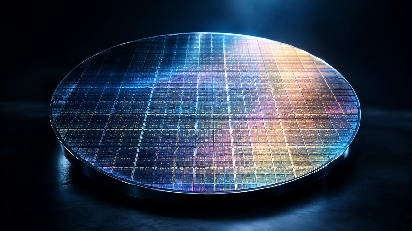
Wafer-Scale Integration (WSE-3) is an advanced semiconductor manufacturing architecture that uses an entire 300-millimeter silicon wafer to create one massive, unified processor, rather than cutting it into hundreds of smaller chips. By keeping all memory, compute, and routing on a single 46,225 mm² piece of silicon, it completely eliminates external networking bottlenecks.
At a Glance
- Concept: Refusing to cut a silicon wafer into little squares, and instead programming the whole giant circle to act as one mind.
- Why it matters: AI models are starving for memory bandwidth. A standard GPU maxes out at 3 TB/s of bandwidth. The WSE-3 delivers 21,000 TB/s because the data never has to squeeze through a physical wire to leave the chip.
- Who uses it: Vanguard AI research labs, the Department of Energy, and cloud hyperscalers seeking ultra-low-latency inference via the new CS-4 platform.
- Biggest takeaway: Creating a chip this big violates the fundamental rule of chipmaking, because one microscopic speck of dust will ruin the chip. Cerebras solved this by building 70,000 extra “spare parts” directly into the silicon to bypass microscopic damage.
In Simple Words
Imagine a massive corporate office where 100,000 employees are trying to finish a massive project together.
In a traditional GPU Cluster, these employees are locked in separate buildings scattered across a city. Whenever they need to share information, they have to put a file in a delivery truck, drive it through city traffic, and drop it off at the other building. Most of their day is wasted waiting for delivery trucks.
Wafer-Scale Integration (WSE-3) puts all 100,000 employees inside the exact same giant, open-concept warehouse. There are no walls, no delivery trucks, and no traffic. If someone needs a file, they just hand it to the person sitting one inch away from them.
Because the “employees” (the transistors) never have to leave the building (the silicon chip), the speed at which they can complete the project increases exponentially.
Why This Matters
For Cloud Architects, Hardware Engineers, and AI VCs, this technology shatters the Memory Wall.
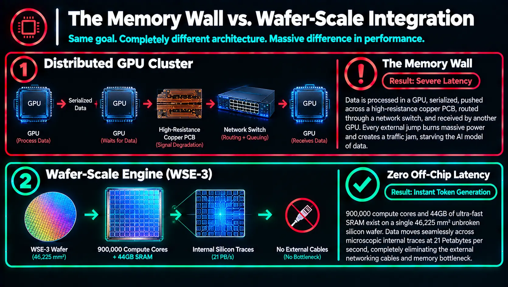
Large Language Models (LLMs) like GPT-4 do not struggle with math; they struggle with memory retrieval. Generating a single word (a token) requires the processor to read massive amounts of data from the memory bank. In traditional architectures, the memory sits outside the processor. Dragging that data across the motherboard is slow and burns massive amounts of electricity. This is known as the “Memory Wall.”
The WSE-3 attacks this wall by putting 44 Gigabytes of ultra-fast SRAM memory directly on the silicon next to the compute cores. It boasts a staggering 21 Petabytes per second (PB/s) of memory bandwidth—roughly 7,000 times faster than the bandwidth of an Nvidia H100 GPU.
Because the WSE-3 does not have to wait for data to be fetched from external memory, it can generate tokens for massive AI models at blinding speeds. In an ecosystem where AI agents and real-time reasoning models demand zero-latency responses, wafer-scale integration provides an insurmountable speed advantage over traditional distributed clusters.
Micro-Insight: In AI inference, compute speed dictates how smart the answer is, but memory bandwidth dictates how fast you get it.
Bypassing the TSMC Reticle Limit
We are witnessing the Rejection of the Reticle Limit.
Since the invention of the microchip, the industry has been bound by the “reticle limit.” This is the maximum size of the rectangular light beam used to print circuits onto silicon (roughly 858 mm²). To make a bigger processor, companies printed multiple chips side-by-side on a round wafer, cut them out with a diamond saw, and wired them back together.
Wafer-Scale integration rejects the saw. By figuring out how to print functional communication lines across the empty scribe lines that separate the reticle squares, engineers turned a fragmented manufacturing process into a monolithic masterpiece. It is the boldest structural leap in semiconductor packaging in fifty years.
How Wafer-Scale Integration Handles Defects
Building a computer chip the size of a dinner plate requires completely rewriting the laws of lithography, defect management, and thermodynamics. Here is the first-principles breakdown of the architecture.
1. The Fundamental Problem: The Physics of Defects
Silicon manufacturing is imperfect. A 300mm silicon wafer takes three months to bake in a fab, undergoing hundreds of chemical baths and light exposures. Inevitably, microscopic dust particles will land on the wafer, destroying the transistors underneath. If you cut the wafer into 100 small chips, you throw away the 5 chips ruined by dust and sell the 95 good ones. But if the entire wafer is one single chip, a single speck of dust theoretically ruins the whole product.
2. The Core Mechanism: Fail-In-Place Redundancy
To make wafer-scale viable, Cerebras invented “Fail-in-Place” architecture. The WSE-3 is divided into 900,000 active AI cores, but the physical silicon actually contains closer to 970,000 cores.
During factory testing, engineers identify the exact cores that were destroyed by dust. They program the chip’s internal communication fabric to treat those broken cores like roadblocks. The data simply takes a one-millimeter detour around the dead core and uses a redundant backup core instead. The chip perfectly heals itself in software.
3. Technical Depth: Cross-Reticle Interconnects
A lithography machine can only print a small square (the reticle) at a time. The WSE-3 is made up of 84 of these squares printed onto the 300mm wafer. Traditionally, there is a dead space between these squares where the saw cuts the chips apart. Cerebras partnered with TSMC to develop a custom fabrication technique that prints thousands of microscopic wires across these dead zones, seamlessly stitching the 84 independent squares into one continuous, 214-Petabit-per-second communication mesh.
Plain-English Takeaway: They tricked the printer into printing the connecting wires in the blank margins of the page, turning 84 separate pages into one giant, connected poster.
4. Technical Depth: Rack-Scale Power Delivery
You cannot plug a chip with 4 trillion transistors into a standard motherboard. The power requirements are violent. Traditional chips receive power through tiny pins on the bottom. The WSE-3 requires its power to be delivered perpendicularly across the entire surface of the wafer simultaneously. Cerebras mounts the wafer against a massive 3D power distribution block that injects up to 30,000 amps of current directly into the face of the silicon, avoiding destructive current spikes.
5. Real-World Consequences: The CS-4 Liquid Cooled Backpack
In mid-2026, the company pushed the thermodynamics even further, unveiling the CS-4 system. This architecture crams three WSE-3 Turbo wafers into a single data center rack, doubling the power delivery per wafer to squeeze out higher clock speeds. To prevent the silicon from instantly melting, the CS-4 utilizes a rear-mounted “Wafer-Scale Backpack.” This self-contained unit pumps direct liquid cooling directly against the power block, dissipating over 140 kW of heat per rack while completely eliminating the noisy, inefficient air fans used in traditional GPU servers.
AI Networking Architectures
Distributed GPU Cluster Latency vs. Wafer-Scale Integration (WSE-3)
LLM Parameter Size
8B Params
AI Compute Architecture
Distributed GPU Cluster
Single Wafer-Scale (WSE)
Token Generation Speed
0 tok/s
Memory Network Latency
0 µs
Off-Chip Comm Loss
0%
Data Routing & Physical Memory Bottlenecks
SYSTEM IDLE
Real-Time Performance Trajectory
Deploying the Cerebras CS-4 in AI Data Centers
Wafer-scale architecture is not just a theoretical experiment; it is actively rewriting the economics of frontier AI deployment.
Ultra-Fast Agentic Inference: Traditional chatbots generate text at human reading speed. But next-generation “Agentic AI” doesn’t just talk to humans; it talks to other AI agents, completing thousands of sub-tasks in the background before delivering a final answer. This requires generating tokens at blinding speeds. The CS-4 platform is currently clocking over 1,000 tokens per second for models exceeding 10 trillion parameters—speeds that distributed GPU clusters mathematically cannot achieve due to physical network latency.
Asteroid Impact & Climate Modeling: The Department of Energy uses wafer-scale engines to run immense, physics-based high-performance computing (HPC) simulations. A simulation of a global asteroid impact creating a tsunami requires moving petabytes of fluid dynamic data simultaneously. By mapping the Earth’s grid entirely onto the 900,000 cores of the WSE-3, the data flows spatially across the chip exactly how water flows across the Earth, achieving exascale-class simulation speeds at a fraction of the power footprint.
Disaggregated Prefill / Decode Racks: Because the WSE-3 is so fast at generating tokens (decoding), it is too valuable to waste on reading the user’s initial prompt (prefilling). Hyperscalers are deploying the CS-4 in a “heterogeneous” setup. They use cheap, traditional accelerators (like AWS Trainium or AMD Helios) to crunch the massive incoming prompt, and then instantly hand the mathematical state over to the WSE-3 to generate the answer. This maximizes the capital efficiency of the entire data center.
The Economics of Wafer-Scale AI Inference
The core strategic consequence of Wafer-Scale Integration is the Simplification of the Data Center Deployments.
Building an AI supercomputer out of 10,000 GPUs is an infrastructural nightmare. It requires buying 10,000 GPUs, thousands of high-end optical transceivers, hundreds of expensive network switches (like InfiniBand or RoCE v2), and miles of fiber-optic cabling. The failure of a single cable can crash the entire training run. The labor required to rack, wire, and test this system takes months.
A CS-4 rack collapses this entire ecosystem. By wrapping the compute, the networking fabric, the memory, and the liquid cooling into a single, pre-assembled 140 kW module, deployment drops from months to hours. You push the rack into the data center, plug in the water hose, plug in the power, and instantly spin up compute power equivalent to hundreds of distributed GPUs.
Advantages
- Zero Off-Chip Latency: All 900,000 cores communicate on the same piece of silicon in a single clock cycle, achieving 214 Petabits per second of internal bandwidth.
- The 44GB SRAM Advantage: SRAM is the fastest memory in existence. A traditional GPU relies on external HBM (High Bandwidth Memory). WSE-3 keeps 44GB of SRAM directly next to the cores, utterly destroying the “memory wall.”
- Simplified Programming: Distributed GPU programming requires complex parallelization frameworks (like MPI or NCCL) to manually break data into chunks to send across cables. WSE-3 allows developers to write code for one giant chip, drastically lowering the software engineering barrier.
- Volumetric Efficiency: A single CS-4 rack replaces dozens of racks of traditional servers and network switches, condensing exaflop-scale computing into a highly concentrated physical footprint.
Limitations
- Absolute Silicon Lock-In: You cannot upgrade a WSE-3. If you want more power or memory, you cannot snap in a new RAM stick; you must buy an entirely new multi-million dollar wafer system.
- Thermal Density Fragility: Pushing 140 kW into a single rack concentrates a massive amount of thermal stress into a very small area. If the direct-to-chip liquid cooling valves fail, the temperature will spike so fast the $3 million wafer could theoretically destroy itself before the safety shutoffs trigger.
- External Memory Expansion: 44GB of SRAM is massive for a single chip, but modern AI models can exceed hundreds of gigabytes in size. Cerebras must connect the wafer to a proprietary external memory box (MemoryX) to hold these massive models, re-introducing a slight latency penalty when swapping layers of the model onto the wafer.
Takeaway: The WSE-3 is a hyper-specialized dragster. It trades the modularity and upgradeability of standard PC architecture for the absolute, unyielding speed of monolithic physics.
Common Misconceptions
Misconception: The chip is perfectly flawless out of the factory.
Reality: It is riddled with physical defects. Producing a 300mm wafer with zero defects is impossible. The genius of the technology is not perfect manufacturing, but the “Fail-in-Place” software that instantly maps and routes around the microscopic damage.
Misconception: It runs the exact same software as an Nvidia GPU.
Reality: Nvidia relies on the CUDA software ecosystem, which is designed for thousands of tiny cores. WSE-3 uses a proprietary dataflow architecture. While compilers map standard PyTorch or TensorFlow code onto the wafer automatically, it operates on fundamentally different mathematical routing beneath the surface.
Misconception: You just plug it into a wall socket.
Reality: A CS-4 rack draws more power than an entire city block of residential homes. It requires specialized, front-side AC/DC modules and heavy-duty facility liquid cooling loops to survive.
What Most People Miss
The disruptive capability of Sparsity Harvesting.
When an AI model runs, roughly 50% to 80% of the numbers in the matrix are zeros (this is called sparsity). Traditional GPUs are bad at dealing with zeros; they often waste time multiplying them anyway because their rigid architecture demands regular blocks of data.
The WSE-3 is a “dataflow” processor. If a data packet contains a zero, the core instantly ignores it and doesn’t fire. It only spends electricity and time on data that actually matters. Because all the cores are connected directly on the silicon, they can pass this sparse data around dynamically. This hardware-level sparsity harvesting gives the wafer a massive, hidden speed multiplier over rigid GPU architectures.
Comparison Table
| Metric | Traditional Cluster (e.g., Nvidia H100) | Wafer-Scale Integration (WSE-3) |
| Chip Size (Silicon Area) | ~814 mm² | 46,225 mm² (Wafer size) |
| Transistor Count | 80 Billion | 4 Trillion |
| On-Chip Memory (SRAM) | 50 Megabytes | 44 Gigabytes (44,000 MB) |
| Memory Bandwidth | 3 Terabytes per second (HBM) | 21 Petabytes per second (SRAM) |
| Interconnect Bottleneck | Copper cables, optical transceivers, switches | Zero (All on-silicon routing) |
Future Outlook
Next 12–24 Months
The era of Disaggregated Rack Heterogeneity. Through 2027, the focus will shift entirely to how Wafer-Scale systems play with others. Data center operators will not buy CS-4 racks to replace their entire GPU fleet. They will deploy them specifically for the “generation” phase of AI inference, pairing them side-by-side with cheaper ASIC racks that handle the initial prompt digestion. The metric of success will be how efficiently the 2 microseconds of latency between the two different architectures is managed over RoCE v2 Ethernet.
Next 3–5 Years
The scaling of 3D Wafer Stacking. By 2030, the 2D surface area of a 300mm wafer will no longer be enough. Hardware architects will begin bonding entire wafers directly on top of each other. This will stack massive sheets of logic directly onto massive sheets of memory, using millions of microscopic vertical Through-Silicon Vias (TSVs) to create a three-dimensional brain. The thermal management required to extract heat from the middle wafer in this 3D sandwich will become the most lucrative engineering challenge in the semiconductor industry.
Next 10 Years
The Post-Reticle Normalization. By the mid-2030s, wafer-scale integration will no longer be an exotic anomaly; it will force the traditional foundry ecosystem (TSMC, Samsung) to standardize equipment for ultra-large dies. As photonics and silicon merge, we will see entire 300mm wafers printed with built-in optical lasers, allowing these giant brains to beam data directly to other wafers across the data center via light, finalizing the transition from distributed computing to massive, monolithic intelligence blocks.
Most Likely Scenario
Wafer-Scale Integration is the ultimate physical solution to the memory wall. While the proprietary nature of the hardware and extreme cooling requirements create friction for legacy data centers, the performance delta in AI inference is simply too large to ignore. As trillion-parameter models become the baseline for the global economy, the sheer thermodynamic and latency advantages of keeping all 4 trillion transistors on the exact same piece of silicon will ensure that Wafer-Scale systems secure a dominant, high-margin foothold at the apex of hyperscale computing.
Key Takeaways
- Traditional AI clusters wire thousands of small GPUs together, creating massive traffic jams and power losses when data travels across the cables.
- Cerebras Wafer-Scale Engine 3 (WSE-3) leaves the entire 300mm silicon wafer intact, resulting in a single chip with 4 trillion transistors and 900,000 cores.
- Because the data never has to leave the silicon, the WSE-3 achieves 21 Petabytes per second of memory bandwidth, utterly obliterating the networking bottleneck.
- To solve the inevitability of manufacturing defects on a chip this big, engineers added 70,000 extra cores. The software automatically routes data around any broken areas in real-time.
- The newly launched CS-4 system packs three of these massive wafers into one rack, using direct liquid cooling to tame 140 kW of power and deliver ultra-low-latency AI token generation.
Glossary
Agentic AI: Next-generation AI models that do not just answer prompts, but actively take actions, break problems into sub-tasks, and communicate with other AI agents rapidly in the background.
Fail-in-Place Redundancy: A manufacturing safety net where a chip is built with extra, spare cores. If a dust particle ruins a core during manufacturing, the software simply builds a detour to a spare core.
HBM (High Bandwidth Memory): External memory chips stacked next to a traditional GPU. While fast, data still has to cross a microscopic bridge to get from the memory to the processor, causing latency.
Memory Wall: The physical bottleneck in modern computing where processors have become so fast that they spend most of their time waiting idly for data to arrive from the slower memory banks.
Reticle Limit: The maximum size of the rectangular light beam used in traditional semiconductor manufacturing, which usually limits chip sizes to roughly 858 mm².
SRAM (Static Random-Access Memory): The fastest type of memory in existence. It is built directly into the processor itself, meaning data is accessed instantly without crossing any external bridges.
Sources
Cerebras Systems: CS-4 Architecture and WSE-3 Technical Specifications
IEEE Solid-State Circuits Society: Wafer-Scale Integration and the Bypass of the Reticle Limit
TSMC Symposium: Advanced Packaging and Defect Management in Ultra-Large Area Silicon
Futurum Research: Hyperscale Disaggregation and the Economics of Wafer-Scale AI Inference
Department of Energy (DoE): Exascale HPC Simulation Scaling on Dataflow Architectures