Advertisement
)
AT A GLANCE
- Concept: Focal Deflection: Pellicles suspend dust millimeters away from the mask to keep shadows out of focus.
- Concept: Extreme Absorption: EUV light destroys almost all physical matter, requiring advanced nanometer-thin membrane engineering.
- Concept: Thermal Expansion: Absorbed light converts instantly to extreme heat, risking catastrophic membrane rupture during commercial printing.
- Concept: Carbon Nanotubes: Engineered carbon mesh provides the exact structural and thermodynamic stability required to survive high-power scanners.
HOW IT WORKS
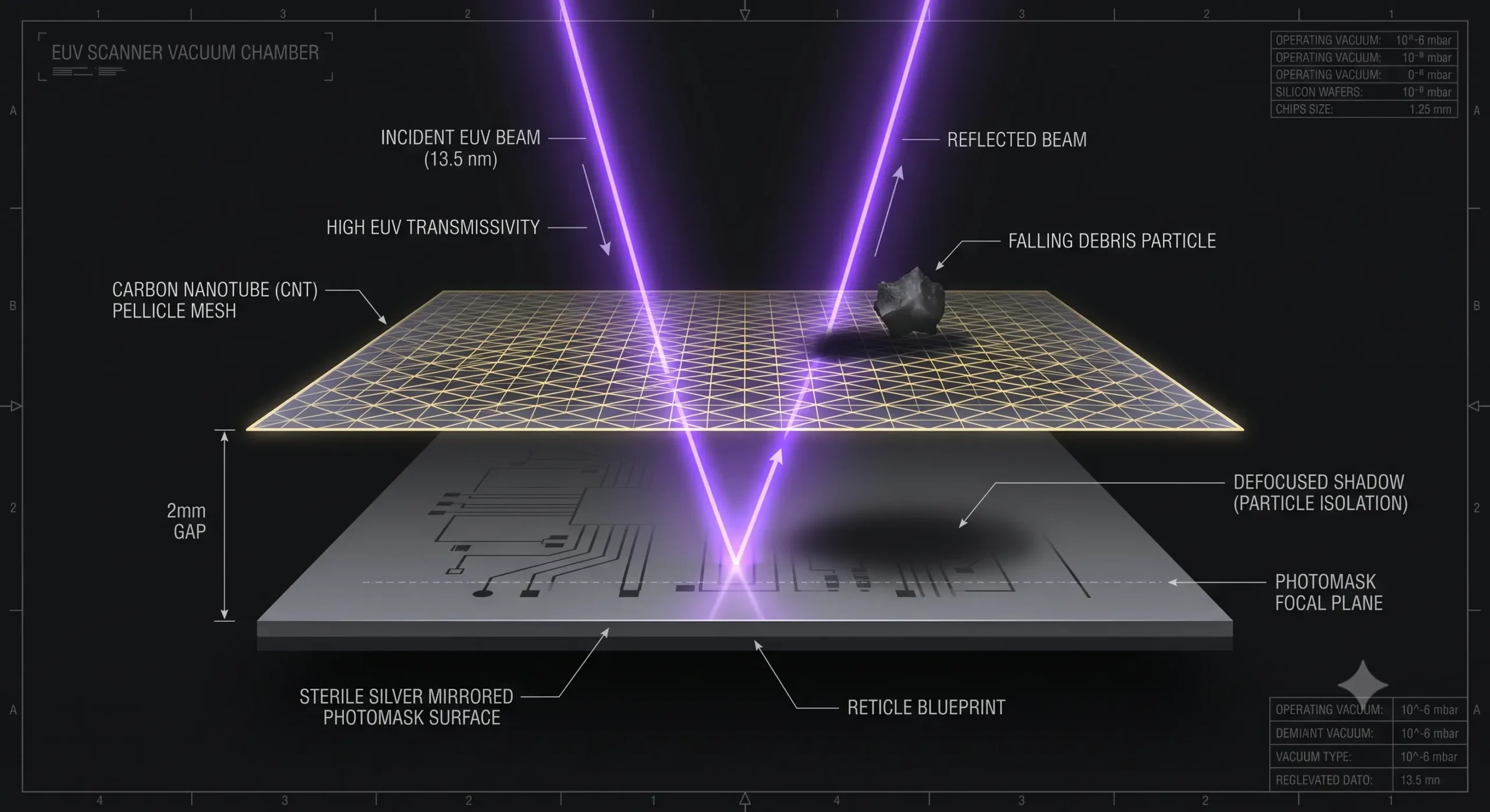
Extreme ultraviolet (EUV) lithography prints sub-2-nanometer transistor gates by bouncing 13.5-nanometer wavelength light off a mirrored photomask. This photomask contains the master blueprint for the entire microchip. If a single particle of dust lands on this mirror, the scanner prints that microscopic shadow onto billions of transistors, instantly destroying the entire silicon wafer.
To prevent this, engineers mount a pellicle—an ultra-thin physical shield—two millimeters above the surface of the mask. Any falling debris lands on the pellicle rather than the mask itself. Because the pellicle sits intentionally out of the optical focal plane, the shadow of the debris blurs completely and never transfers onto the silicon.
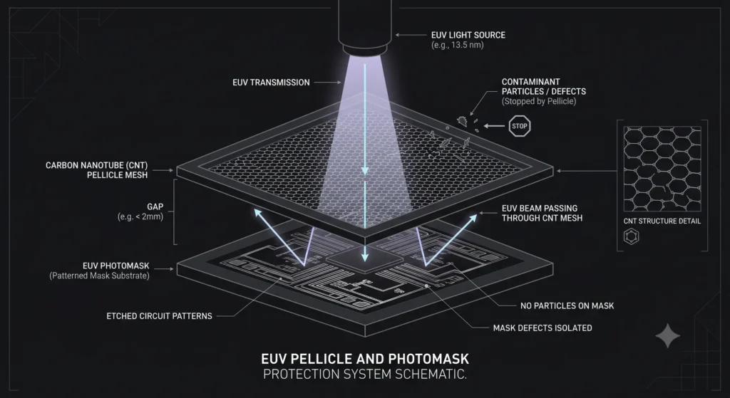
Designing this shield requires defeating extreme optical physics. Standard glass pellicles used in older lithography instantly absorb EUV light, vaporizing the glass. A viable EUV pellicle must be less than fifty nanometers thick to guarantee at least 90 percent light transmission.
At these atomic dimensions, thermal management dictates structural survival. The membrane absorbs roughly 10 percent of the massive EUV energy, converting it directly into heat. Because the membrane sits in a pure vacuum chamber, it cannot rely on convective air cooling and must dissipate heat entirely through thermal radiation.
The radiative cooling capacity follows the Stefan-Boltzmann law:
$$P = \epsilon \sigma A (T^4 – T_0^4)$$
Where P is the net radiated power, ε (epsilon) is the emissivity of the carbon nanotube mesh, σ (sigma) is the Stefan-Boltzmann constant, A is the radiating surface area, and T is the absolute temperature. Engineers rely on the high emissivity of carbon nanotubes to rapidly shed heat before the membrane exceeds its mechanical melting point.
WHY IT MATTERS NOW
Foundries face a severe productivity constraint as they push toward angstrom-era manufacturing. To make 2-nanometer nodes economically viable, chipmakers must expose wafers faster to offset massive capital depreciation costs. ASML is upgrading its High-NA scanners to output 600 watts of source power to achieve these required throughput velocities.
This extreme power output pushes legacy polysilicon pellicles past their physical breaking point. At 600 watts, traditional membranes overheat, warp, and spontaneously rupture inside the scanner. A ruptured pellicle blasts microscopic debris across the multi-million-dollar optical system, forcing the entire fabrication line to halt for weeks of forensic cleaning.
TSMC and Intel cannot risk high-volume commercial production without indestructible defect isolation. If a foundry attempts to print chips without a pellicle, they must spend hours inspecting the photomask for debris after every few hundred exposures. This inspection downtime destroys the unit economics of a high-volume leading-edge fabrication facility.
The chemical industry currently dictates this lithographic speed limit. A single Japanese company, Mitsui Chemicals, controls the commercialization of the carbon nanotube pellicle architectures required to survive these 600-watt environments. This hyper-concentrated supply chain grants a mid-sized material science firm veto power over the deployment schedules of global semiconductor production.
WHAT MOST PEOPLE MISS
General technology analysis obsessively tracks the delivery schedules of massive ASML photolithography machines, assuming the scanner is the only variable in Moore’s Law. They treat the actual photomask as a static, solved component.
They miss the severe material thermodynamics governing high-volume manufacturing. Carbon nanotube pellicles operate at temperatures exceeding 600 degrees Celsius in a pure vacuum while experiencing continuous mechanical vibration. The true engineering moat of next-generation computing is not just generating extreme ultraviolet light, but synthesizing a membrane that can withstand that light without instantly turning into plasma.
THE TRAJECTORY
Next 12–36 Months: Foundries will fully integrate first-generation carbon nanotube pellicles into their baseline 2-nanometer production flows. This integration will immediately boost wafer yield consistency by eliminating the intermittent inspection halts previously required for unprotected masks.
Next Five Years: Chemical suppliers will commercialize metallic-coated graphene mesh structures. These composite membranes will push transmission rates past 95 percent, recovering the optical efficiency lost by the physical presence of the carbon shield.
Next Ten Years: The industry will move toward dynamic, active-cooling frames. Engineers will circulate microscopic volumes of liquid helium through the outer border of the pellicle structure, aggressively pulling heat from the carbon mesh to enable future 1,000-watt source power milestones.
What Could Go Wrong: A severe supply chain disruption in the highly specialized manufacturing of uniform carbon nanotubes would stall global logic scaling. Without access to these specific thermal shields, foundries would be forced to run their expensive 600-watt scanners at half capacity to prevent catastrophic membrane failure.
Most Likely Outcome: The carbon nanotube pellicle will establish itself as the mandatory, non-negotiable consumable of the High-NA EUV era. The market will remain fiercely guarded by a strict oligopoly of advanced material science corporations, cementing their status as the hidden gatekeepers of high-performance artificial intelligence hardware.
KEY TERMS
- Photomask: A highly precise, mirrored template containing the physical layout of the microscopic circuits required to manufacture a semiconductor chip.
- Pellicle: A thin, transparent membrane stretched across a frame to protect a photomask from falling debris during the lithography process.
- Extreme Ultraviolet (EUV): An ultra-short 13.5-nanometer wavelength of light used to print the smallest transistor features in modern semiconductor manufacturing.
- Carbon Nanotube: A cylindrical molecular structure consisting entirely of carbon atoms, chosen for its extreme tensile strength and superior thermal conductivity.
- High-NA Lithography: The next generation of semiconductor printing technology that uses a larger numerical aperture lens system to print finer structural geometries.
SOURCES
- ASML — EUV Pellicle Technology and High-NA Transmission Requirements
- Mitsui Chemicals — Carbon Nanotube Pellicle Commercialization for Advanced Lithography
- TSMC — Defect Reduction Strategies and Mask Inspection in Sub-3nm Nodes
- SPIE (International Society for Optics and Photonics) — Thermal and Mechanical Stability of Carbon Nanotube EUV Pellicles