Advertisement
)
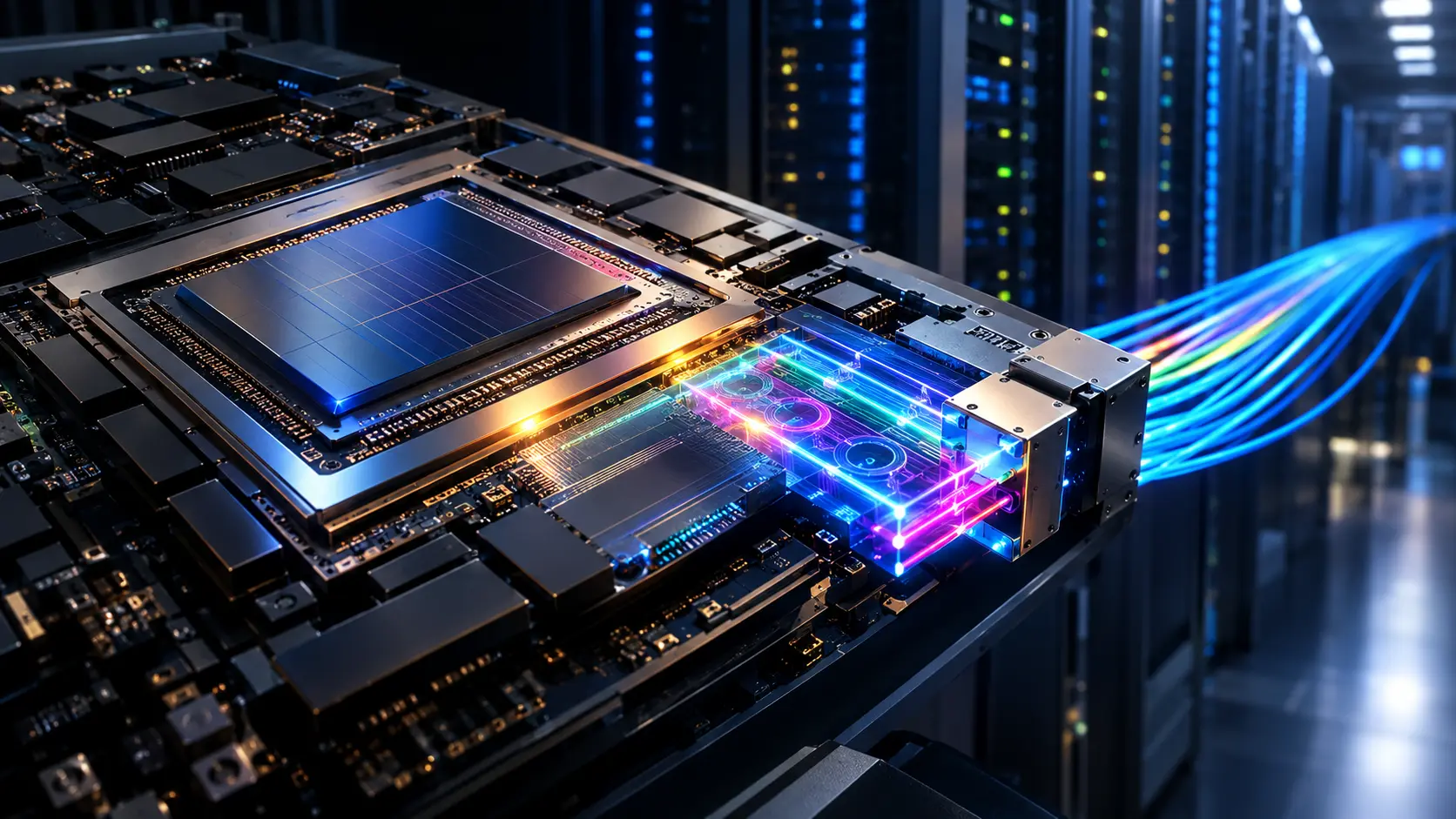

If you walk into a modern artificial intelligence data center, you will notice a bizarre physical problem: the server racks are choking on their own cables. To train a massive AI model, thousands of GPUs must talk to each other in perfect unison. They currently do this through dense bundles of copper wire. But at the blazing speeds required by modern AI, copper acts like a resistor. Squeezing massive amounts of data through copper generates severe electrical friction, bleeding power as heat. To combat this, engineers have to make the cables thicker and shorter. Today, backend GPU network cables are so thick and heavy they literally block the cooling fans, and they can only reach a few meters before the electrical signal completely dies.
Why should you care right now? Because the physics of copper have flatlined, and the semiconductor industry is executing a radical pivot to light. Hardware companies are now embedding microscopic optical lasers directly onto the silicon chip itself. Known as Optical I/O, this technology rips out the power-hungry copper transmitters and replaces them with silicon photonics. By converting data into light at the atomic level, AI chips can communicate at near-infinite bandwidth across the entire data center with practically zero heat, fundamentally dismantling the hardware barriers throttling the next generation of artificial intelligence.
What are Optical I/O Chiplets?
Optical I/O chiplets are miniaturized silicon photonics modules integrated directly onto the same package as a primary processor (like a GPU). They convert electrical data signals into light instantaneously at the chip level, bypassing traditional copper wiring to enable high-bandwidth, ultra-low-latency, and energy-efficient communication across massive computing clusters.
At a Glance
- Concept: Replacing the electrical copper “mouth” and “ears” of a microchip with lasers and light sensors.
- Why it matters: AI clusters are starving for data. Copper wiring uses too much power and can’t carry enough data over long distances. Light carries exponentially more data using a fraction of the power.
- Who uses it: Hyperscale cloud providers, AI supercomputer architects, and vanguard photonic companies like Ayar Labs, Broadcom, and Intel.
- Biggest takeaway: This is not optical computing. The chip still thinks using electricity. Optical I/O is simply about moving that electrical thought from one chip to another via light, without using a heavy copper bridge.
In Simple Words
Imagine you need to send millions of letters from New York to London.
Using Copper Wiring is like hiring a fleet of heavy diesel trucks to drive the letters onto cargo ships. It is slow, the trucks burn massive amounts of fuel (power), and they take up a ton of physical space on the highway. If you want to send more letters, you just have to buy more trucks and widen the highway, until the entire city is paralyzed by traffic.
Using Optical I/O is like converting those letters into a digital email and beaming them across a fiber-optic cable in a fraction of a second.
In the past, the machine that turned the letters into emails was a huge, clunky box sitting far away from the sender (pluggable transceivers). Today, engineers have shrunk that machine down to the size of a grain of rice and glued it directly to the processor. The chip spits out light instead of electricity, solving the traffic jam permanently.
Why This Matters
For Cloud Architects, Hardware Engineers, and AI Investors, Optical I/O solves the SerDes Power Wall.
Inside every modern chip, there is a block of circuitry called the SerDes (Serializer/Deserializer). Its only job is to take the parallel data inside the chip, line it up single-file, and blast it out over a copper wire to another chip.
As GPUs have become exponentially faster, they process data faster than the SerDes can push it out. To compensate, engineers increase the speed of the SerDes. But pushing electricity through copper at 200 Gigabits per second (Gbps) is thermodynamically brutal. Today, the SerDes consumes up to 30% of the entire power budget of an advanced network switch or GPU.
We are reaching a point where we cannot supply enough electricity to power both the actual “thinking” parts of the GPU and the “talking” parts of the GPU. By replacing the electrical SerDes with an Optical I/O chiplet, the power required to transmit a bit of data drops by up to 80%. This reallocates massive amounts of electricity and cooling capacity back to the AI cores, instantly increasing the raw intelligence of the cluster.
Micro-Insight: In modern computing, processing the data is cheap; moving the data is expensive. Optical I/O makes moving data virtually free.
The Disaggregation of AI Data Centers
We are witnessing the Disaggregation of the Data Center.
Because copper cables can only transmit high-speed data for about two meters before the signal dies, hardware architects are forced to cram GPUs, CPUs, and Memory as closely together as physically possible inside the same metal rack.
Light does not degrade over a few meters. An optical signal can travel 2 kilometers with the exact same power consumption and latency as it takes to travel 2 millimeters. This shatters the physical constraints of the server rack. A cloud architect can put all the GPUs in one room, all the memory in another room, and connect them via Optical I/O, treating the entire warehouse-scale data center as if it were one single, massive motherboard.
How Optical I/O Chiplets Use Silicon Photonics
Translating an electrical thought into a beam of light inside a piece of silicon requires absolute mastery over nanoscale photonics. Here is the first-principles breakdown of the architecture.
1. The Fundamental Problem: Pluggable Optics
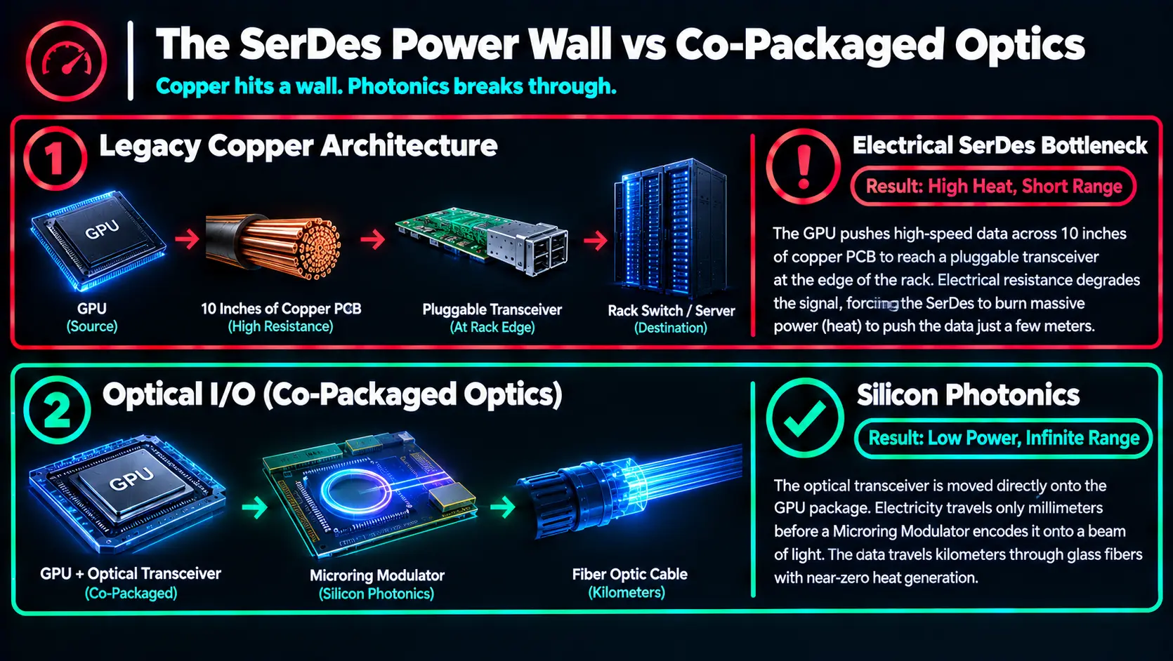
Data centers already use fiber optics for long distances. But traditionally, the laser transceivers are “pluggable”—they sit at the edge of the server rack. The GPU must still push an electrical signal across a copper circuit board for 10 inches just to reach the laser. At modern AI speeds, driving a signal across 10 inches of copper ruins the signal integrity and burns massive amounts of power.
2. The Core Mechanism: Co-Packaged Optics (CPO)
To eliminate that 10-inch copper journey, engineers use Co-Packaged Optics (CPO). They take the optical transceiver and package it onto the exact same piece of silicon substrate as the GPU. The electrical signal only has to travel a few millimeters to reach the optical chiplet, virtually eliminating electrical loss.
3. Technical Depth: Microring Modulators (MRMs)
How does a chiplet turn electricity into light? It uses a Microring Modulator. Imagine a microscopic racetrack made of silicon sitting next to a straight optical fiber. Continuous light flows through the fiber. When the GPU sends an electrical “1”, it changes the refractive index of the racetrack, causing the light to divert into the ring and dim the main fiber. When the GPU sends a “0”, the light passes straight through. The MRM acts as a microscopic shutter, blinking billions of times a second to encode data into the light beam.
Plain-English Takeaway: A microring modulator is just an impossibly fast, atomic-scale flashlight switch. It converts the electrical 1s and 0s of the computer chip into flashes of light.
4. Technical Depth: Dense Wavelength Division Multiplexing (DWDM)
If you only use one color of light, you can only send one stream of data. Optical I/O uses DWDM to send multiple colors (wavelengths) of light through the exact same fiber simultaneously. By tuning different Microring Modulators to react only to specific colors (e.g., Red, Blue, Green), a single microscopic glass fiber can carry terabits of data at the same time without the streams ever mixing or colliding.
5. Real-World Consequences: The Off-Package Laser
Lasers hate heat. GPUs generate massive amounts of heat. If you put the laser directly next to the GPU, the laser will quickly degrade and die. Leading companies like Ayar Labs solve this by separating the architecture. They put the Microring Modulator (which likes heat) on the chiplet (the TeraPHY). They put the actual laser light source (the SuperNova) on a separate module plugged into the wall, far away from the hot GPU. The remote laser shines continuous, blank light into the chiplet via a fiber, and the chiplet simply modulates it.
Optical I/O vs. Copper SerDes Simulator
Overcoming High-Frequency Attenuation & the SerDes Power Wall in AI Clusters
Interconnect Distance
2.0 m
Transmission Fabric
Copper SerDes
Optical I/O (CPO)
Energy Consumption
18.5 pJ/bit
Signal Integrity (Eye Opening)
82.0%
Thermal Dissipation
Nominal (34°C)
Co-Packaged Silicon Interface & Physical Interconnect
ELECTRICAL SERDES ACTIVE
Real-Time Signal Integrity & Energy Efficiency vs. Distance
Commercial Deployments of Co-Packaged Optics
Optical I/O is rapidly exiting stealth R&D and entering the highest tiers of global computing architecture.
AI Supercomputing Networks (NVLink/CXL): Nvidia’s NVLink allows GPUs to share memory, but it is heavily constrained by copper cable lengths, limiting a single cluster to a few hundred GPUs in tightly packed racks. By replacing the electrical pins with Optical I/O chiplets, hardware architects can stretch high-speed memory fabrics across thousands of GPUs spread across massive data halls, allowing them to train multi-trillion-parameter models as if they were a single massive brain.
Disaggregated Rack Architecture: In a traditional server, the CPU, Memory, and Storage are bolted onto the same motherboard. If you need more memory, you have to buy a whole new server. Optical I/O enables PCIe and CXL (Compute Express Link) over optics. This allows engineers to build entire racks that are only memory, and connect them optically to racks that are only CPUs. The processors can pull data from a memory bank across the room at the exact same speed as if it were soldered next to it.
Aerospace and Defense Payloads: Weight and electromagnetic interference (EMI) are critical bottlenecks in fighter jets and satellites. Thick copper cables are heavy and susceptible to enemy radar and electronic warfare jamming. Optical fibers are feather-light and completely immune to EMI. Swapping copper for Optical I/O in military sensor fusion platforms slashes aircraft weight and secures data transmission against electromagnetic attacks.
Economic & Strategic Impact
The core strategic consequence of Optical I/O is the Eradication of the Distance Penalty.
In the digital economy, geography dictates capability. The layout of a data center is entirely governed by how far an electrical signal can travel before it degrades. This forces companies to spend billions engineering exotic cooling systems just so they can pack chips close enough together to talk.
Optical I/O removes distance as an engineering variable. When it costs the same amount of power to send a terabyte of data two meters as it does to send it two kilometers, data centers no longer need to be hyper-dense, melting boxes of silicon. They can be distributed seamlessly. This fundamentally lowers the Capital Expenditure (CapEx) required for thermal management and allows cloud providers to scale AI infrastructure without being bottlenecked by the physical geometry of a server rack.
Advantages
- Bandwidth Density: A single microscopic optical fiber can carry the same amount of data as dozens of thick, heavy copper cables, clearing physical congestion inside the server.
- Distance Agnosticism: Light does not degrade over data-center distances, allowing high-speed memory pooling across completely separate racks and rooms.
- Massive Power Reduction: Converting electricity to light on-package slashes the picojoules-per-bit (pJ/bit) energy cost by up to 80% compared to driving a signal across copper circuit boards.
- Pin Efficiency: Modern GPUs have thousands of electrical pins underneath them, and they are running out of physical space. Optical I/O multiplexes data, drastically reducing the number of physical pins required for networking.
Limitations
- Packaging Complexity: Integrating silicon photonics onto the same organic substrate as a massive, heat-generating GPU requires sub-micron alignment precision. If the microscopic glass fiber shifts by even a fraction of a millimeter during manufacturing, the light is lost.
- The Laser Reliability Problem: Lasers eventually burn out. If the laser is permanently glued inside the GPU package and it dies, a $30,000 GPU becomes a brick. This is why decoupling the laser into a replaceable, off-package module is mandatory for commercial scaling.
- Ecosystem Inertia: The entire global electronics supply chain is built around copper soldering, printed circuit boards (PCBs), and electrical testing. Transitioning assembly lines to handle delicate optical fibers requires massive CapEx retooling by companies like TSMC and Foxconn.
Takeaway: The physics of Optical I/O are flawless. The challenge is entirely mechanical. Splicing glass to silicon at a scale of millions of units per year without breaking the glass is a brutal manufacturing hurdle.
Common Misconceptions
Misconception: Optical I/O means we are building “Optical Computers.”
Reality: The actual computation (the math) is still done using electrons moving through silicon transistors. Optical I/O is strictly about communication—moving the result of that math to the next chip.
Misconception: Copper is completely dead.
Reality: Copper will always be used for very short distances (e.g., inside the chip package itself, or from the GPU to the High-Bandwidth Memory stacked directly on top of it). Optical I/O replaces the copper that leaves the chip package.
Misconception: Fiber optics in data centers is a new idea.
Reality: Data centers have used fiber optics for decades between switches. What is new is where the electricity is converted to light. It used to happen far away from the chip; now, it happens inside the chip itself (Co-Packaged Optics).
What Most People Miss
The disruptive capability of The Analog Transition.
When analysts look at Optical I/O, they assume it functions exactly like digital copper, just faster. What they miss is that light is inherently an analog wave.
In traditional copper SerDes, massive amounts of processing power are spent doing Digital Signal Processing (DSP)—cleaning up the messy electrical signal so the receiving chip can read the 1s and 0s. Because light moving through fiber doesn’t experience the same interference and distortion as electricity through copper, Optical I/O chiplets can often bypass heavy DSP entirely. This “direct drive” optical signaling strips out massive amounts of latency, allowing chips to communicate in pure, raw analog bursts with virtually zero processing delay.
Comparison Table
| Metric | Copper Wiring (Electrical SerDes) | Pluggable Optics (Traditional Fiber) | Optical I/O Chiplets (CPO) |
| Data Translation Point | N/A (Stays electrical) | Edge of the server rack | Directly on the GPU package |
| Max Distance | < 2 Meters (at high speed) | 2+ Kilometers | 2+ Kilometers |
| Power Efficiency | Poor (High heat) | Moderate | Exceptional (< 5 pJ/bit) |
| Bandwidth Density | Low (Thick cables) | Moderate | Extremely High (DWDM) |
| Latency | Low | High (Due to heavy DSP) | Ultra-Low (Direct drive) |
Future Outlook
Next 12–24 Months
The era of Proprietary AI Cluster Deployments. Through 2027, Optical I/O will not be a commodity you buy off the shelf. It will be custom-integrated into the flagship AI supercomputers built by Nvidia, Google (TPU), and AMD. The primary focus is validating the reliability of remote laser sources (External Laser Sources, ELS) in high-vibration, high-heat data center environments, ensuring they can survive continuous multi-month LLM training runs.
Next 3–5 Years
The scaling of CXL over Optics. By 2030, the Compute Express Link (CXL) protocol will fully merge with Optical I/O. This will shatter the traditional server motherboard architecture. Hyperscalers will begin deploying completely disaggregated racks, where vast pools of memory and storage are shared dynamically across thousands of optical channels. If a GPU needs more memory for 10 seconds, it will borrow it from a rack 50 meters away at the speed of light.
Next 10 Years
The Monolithic Photonic Era. By the mid-2030s, the current “chiplet” approach—where the optical silicon is glued next to the electronic silicon—will evolve. Foundries will master monolithic integration, etching the Microring Modulators and optical waveguides directly into the same piece of primary silicon alongside the logic transistors. Copper pins for data transmission will be entirely eliminated from high-end silicon, relegating copper strictly to power delivery.
Most Likely Scenario
Optical I/O is the mandatory lifeline for the artificial intelligence industry. The thermal and geometric limits of pushing electricity through copper have been reached. While the mechanical friction of scaling sub-micron optical packaging will delay broad consumer adoption, the sheer economic necessity of feeding data to AI accelerators guarantees its success in the hyperscale market. By converting data to light at the package level, the industry secures the bandwidth necessary to scale AI models into the next decade.
Key Takeaways
- To scale AI models, thousands of GPUs must talk to each other. Currently, they use copper wires, which consume massive amounts of power and generate crippling heat at high speeds.
- Optical I/O replaces the electrical transmitters on a microchip with tiny silicon photonics (lasers and modulators), blasting data across the data center via light.
- This is achieved through Co-Packaged Optics (CPO), moving the light-conversion engine off the edge of the server rack and directly onto the processor itself.
- By using Microring Modulators and different colors of light (DWDM), a single microscopic fiber can carry terabits of data, replacing thick, heavy copper bundles.
- Optical I/O eliminates the “distance penalty.” An AI chip can communicate with memory across the room with the exact same power and speed as if it were glued right next to it.
Glossary
Co-Packaged Optics (CPO): The advanced manufacturing technique of placing optical transceivers on the exact same substrate (package) as the main processing chip, rather than at the edge of the circuit board.
DWDM (Dense Wavelength Division Multiplexing): A technology that puts data from different sources together on an optical fiber, with each signal carried on its own separate light wavelength (color).
Microring Modulator (MRM): A microscopic, ring-shaped silicon structure that alters its refractive index when electricity is applied, acting as an ultra-fast shutter to encode digital data onto a continuous beam of light.
Optical I/O: (Input/Output). The overarching architecture of using light, rather than electrical copper pins, for a microchip to communicate with the outside world.
Pluggable Transceiver: The traditional, thumb-drive-sized modules plugged into the front of a server that convert the server’s electrical signals into optical signals for long-distance travel.
SerDes (Serializer/Deserializer): The electrical circuit inside a chip that takes parallel internal data and lines it up single-file to be blasted across a copper wire.
Sources
Ayar Labs: In-Package Optical I/O and the TeraPHY Architecture
Broadcom: Co-Packaged Optics (CPO) for Hyperscale Data Centers
IEEE Solid-State Circuits Society: The Power Wall of Copper SerDes in Scaling AI Clusters
LightCounting: Market Forecast for Silicon Photonics and Optical Interconnects
Open Compute Project (OCP): Hardware Disaggregation and CXL over Optics