Advertisement
)

AT A GLANCE
- Concept: Frontside Congestion: Legacy chip designs force both power lines and data signals to share the same cramped physical layer.
- Concept: IR Drop: As power travels through dozens of microscopic routing layers, resistance severely degrades the voltage.
- Concept: Buried Power Rails: Engineers etch trenches directly into the silicon substrate to sink power lines below the active transistors.
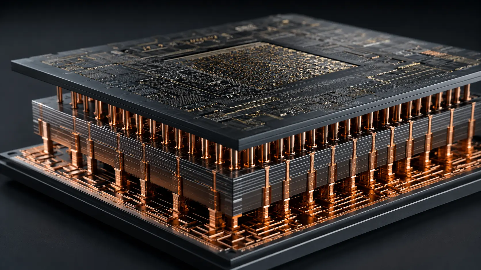
- Concept: Nano-Vias: Microscopic vertical copper pillars puncture the silicon block to connect the back-side power grid to the front-side logic.
HOW BACKSIDE POWER DELIVERY WORKS
For sixty years, semiconductor foundries manufactured microprocessors like a single-story city. Engineers placed billions of transistors on the flat silicon substrate, then built a complex, multi-story skyscraper of copper wiring directly on top of them. This top layer handles both the data signals communicating logic and the electrical power keeping the chip alive.
As foundries shrink transistors below 2 nanometers, this shared front-side architecture physically collapses. Pushing massive electrical currents through dozens of increasingly narrow metal layers creates severe electrical resistance. This resistance causes a phenomenon known as IR drop, where the voltage mathematically degrades before it ever reaches the transistor.
Backside power delivery solves this physics problem by separating the power grid from the data network. Foundries physically flip the silicon wafer upside down during manufacturing. They grind away the excess silicon bulk until the wafer is microscopic, exposing the underside of the transistor layer.
Engineers then construct an entirely new, heavy-gauge copper power grid on this freshly exposed backside. They connect this new grid to the active transistors using Buried Power Rails (BPR) and Nano-Through-Silicon Vias (nTSVs).
This architecture allows electricity to travel straight up into the transistor from the bottom. It completely bypasses the dense, fragile web of data signal wires sitting on top, providing clean, uncorrupted power directly to the logic gates.
WHY IT MATTERS NOW
The artificial intelligence industry demands processing nodes capable of consuming hundreds of watts of continuous power. Standard frontside delivery networks physically cannot feed sufficient voltage to dense, multi-chip AI accelerators without melting the surrounding signal wires. Backside power delivery permanently removes this thermal and electrical bottleneck.
By moving the power grid to the back of the wafer, foundries free up massive amounts of physical space on the front side. Chip designers suddenly reclaim up to thirty percent of the routing capacity previously occupied by thick power cables.
This reclaimed geometry allows engineers to pack logic gates tighter. It shortens the physical distance data must travel across the chip, instantly increasing calculation speeds while simultaneously reducing the energy required to push the signal.
Intel bet its entire foundry survival strategy on this exact mechanic. The company developed PowerVia, introducing backside power delivery ahead of its primary competitors. This aggressive engineering maneuver aims to bypass TSMC by offering hyperscale cloud providers a structurally superior electrical footprint for their next-generation AI silicon.
The economic consequences dictate the timeline of the sub-2nm node transition. Manufacturing a backside network requires extreme precision in wafer thinning and double-sided alignment. Foundries that master this geometry will monopolize the high-performance computing market, as legacy frontside chips simply will not boot up under the extreme voltage demands of future data centers.
WHAT MOST PEOPLE MISS
Hardware commentators frequently obsess over the exact shape of new transistors, debating the merits of FinFETs versus Gate-All-Around (GAA) nanosheets. They completely ignore that a better transistor is useless if you cannot physically deliver uncorrupted voltage to it.
The true barrier to sub-2nm scaling is not drawing a smaller switch; it is managing the extreme physical stress of double-sided manufacturing. To build a backside grid, robots must bond the ultra-thin, fragile silicon wafer to a temporary glass carrier just to keep it from shattering while machines polish the back.
Any microscopic deviation in this mechanical bonding process instantly destroys a $20,000 wafer. The semiconductor moat is no longer defined strictly by lithography limits, but by the physical metallurgy and mechanical engineering required to flip and grind silicon at atomic tolerances.
THE TRAJECTORY
Next 12–36 Months: Major foundries will scale initial production of backside power nodes. Intel will deploy its 20A node utilizing PowerVia, while TSMC prepares its N2P architecture, forcing high-end smartphone and GPU designers to rewrite their physical layout algorithms entirely.
Next Five Years: The integration of backside active components. Engineers will stop using the rear of the wafer solely for power lines and begin etching deep trench capacitors and voltage regulators directly into the backside silicon, moving power management microscopically close to the logic gates.
Next Ten Years: True 3D monolithic integration. Foundries will use the backside power grid as a foundation to physically stack a second, completely separate layer of transistors on the bottom of the wafer. This creates a two-faced computing die that doubles computational density without increasing the chip’s planar footprint.
What Could Go Wrong: Wafer warpage during extreme thermal cycling. The copper power grid on the back expands at a different physical rate than the logic grid on the front. If the chip runs a heavy AI workload, the mismatched thermal expansion can physically bend the silicon die, snapping the nano-vias and permanently bricking the processor.
Most Likely Outcome: Backside power delivery will become the mandatory architectural foundation for all high-performance silicon. The geometry of standard frontside routing simply cannot sustain the voltage requirements of next-generation atomic scaling.
KEY TERMS
- IR Drop: The mathematical reduction in voltage that occurs as electrical current pushes through the physical resistance of highly congested copper wiring.
- Nano-Through-Silicon Via (nTSV): A microscopic, vertical copper pillar etched directly through the silicon substrate to connect the front and back sides of a microchip.
- Buried Power Rail (BPR): A conductive trench embedded deep within the lower layers of the silicon bulk, acting as a direct electrical socket for the transistors above it.
- Gate-All-Around (GAA): A modern transistor design where the conductive gate completely surrounds the silicon channel on all four sides to prevent electrical leakage.
- Frontside Routing: The traditional method of manufacturing where both power delivery cables and data communication wires stack exclusively on top of the silicon die.
SOURCES
- IEEE International Electron Devices Meeting (IEDM) — Backside Power Delivery and Buried Power Rail Integration
- IMEC — Overcoming IR Drop through Extreme Wafer Thinning and Backside Power Networks
- Intel Corporation — PowerVia: Intel’s Architecture for Backside Power Delivery
- TSMC (Taiwan Semiconductor Manufacturing Company) — N2P Node Architecture and Advanced Power Distribution Mechanics