Advertisement
)
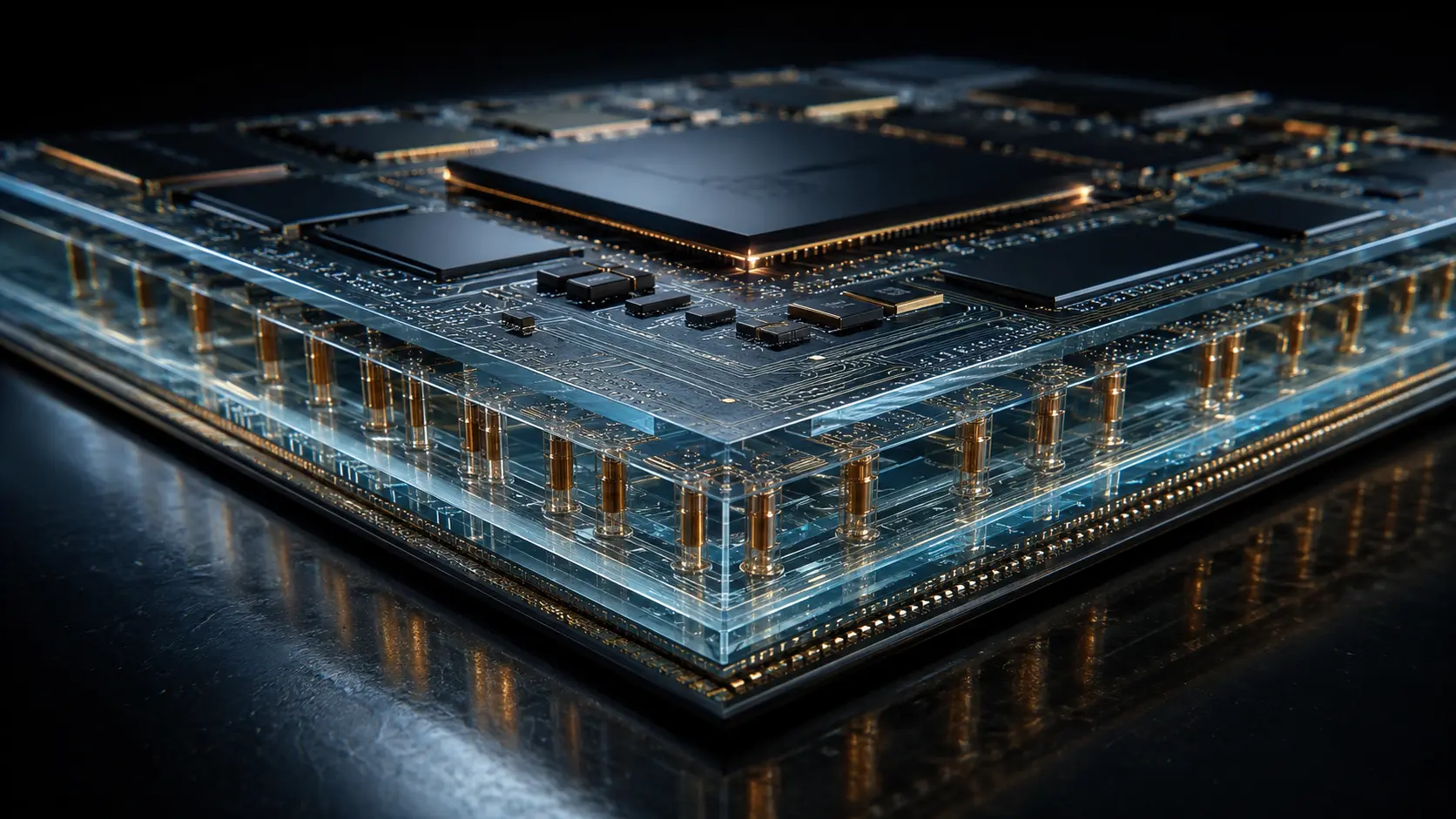

A modern artificial intelligence super-chip—packing over 100 billion transistors—draws over 1,000 watts of power. It runs so relentlessly hot that the green, organic plastic circuit board sitting beneath it literally warps, bends, and bows like a piece of warped plywood left out in the rain. When this microscopic bending occurs, the tens of thousands of fragile, microscopic solder bumps connecting the chip to the board instantly snap. The $40,000 AI processor is destroyed before it ever leaves the factory. For a decade, the semiconductor industry has fought this physical limit, trying to build larger and heavier logic architectures on top of flimsy, thermal-sensitive plastic resins. They have officially hit the wall.
Why should you care right now? Because the infrastructure of the global digital economy is transitioning from plastic to glass. Prompted by Intel’s historic roadmap pivot, the world’s premier chipmakers are abandoning organic laminates and investing billions in Glass Core Substrates (GCS). By mounting AI chips directly onto microscopic sheets of highly modified, conductive glass, engineers are solving the fatal thermal warping bottleneck while simultaneously unlocking the electrical speeds necessary for next-generation optical networking. It is a complete architectural reboot of how computers are physically constructed, enabling the next ten years of artificial intelligence scaling.
What are Glass Core Substrates (GCS)?
Glass Core Substrates (GCS) are advanced semiconductor packaging materials that replace traditional organic resin cores with high-purity glass. They feature a Coefficient of Thermal Expansion (CTE) that perfectly matches silicon, preventing high-heat warpage, while utilizing microscopic Through-Glass Vias (TGVs) to route ultra-high-speed electrical signals between densely packed chiplets and memory modules.
At a Glance
- Concept: Discarding the standard green, plastic “motherboard” material inside a microchip package and replacing it with a rigid, ultra-smooth sheet of glass.
- Why it matters: Glass doesn’t bend when it gets hot, and it doesn’t absorb electrical signals. This allows engineers to build AI packages that are 50% larger and run twice as fast.
- Who uses it:Mega-foundries (TSMC, Intel, Samsung) and specialized substrate manufacturers (Absolics, Ibiden, Corning, SCHOTT) racing to feed the AI hyperscaler market.
- Biggest takeaway: You cannot simply drill a hole in glass to run a wire through it; the glass shatters. The industry had to invent specialized femtosecond lasers that instantly vaporize microscopic columns through the glass to create the wiring paths.
In Simple Words
Imagine you are trying to build a massive, complex city of skyscrapers (the AI chips and memory) right next to each other.
For the last twenty years, the semiconductor industry has been building these cities on top of a giant swamp (organic plastic substrates). As long as the city was small, the swamp held up fine. But now, the AI cities are so heavy, massive, and generate so much heat that the swamp is sinking and shifting. The roads connecting the skyscrapers (the microscopic wires) are snapping because the ground underneath them is buckling.
Glass Core Substrates represent a decision to stop building on the swamp, and start building on solid bedrock.
Glass is perfectly flat, incredibly rigid, and does not shift or bend when exposed to extreme heat. Because the foundation is perfectly stable, engineers can build the skyscrapers much closer together and run perfectly straight, ultra-fast subway lines (Through-Glass Vias) directly through the bedrock, connecting everything at speeds that were physically impossible on the muddy plastic.
Why This Matters
For Hardware Investors and Cloud Architects, the commercialization of GCS is the definitive key to defeating the “Reticle Limit” constraint of AI packaging.
Currently, the size of an AI processor is limited by the organic substrate’s inability to stay flat when large silicon interposers are bonded to it. Glass inherently resists this warpage.Furthermore, the glass substrate market is projected to surge from roughly $650 million in 2024 to over $8 billion by 2030, a blistering Compound Annual Growth Rate (CAGR) driven entirely by High-Performance Computing (HPC) demand. The companies that successfully secure High-Volume Manufacturing (HVM) yields on glass over the next 24 months will effectively monopolize the physical supply chain for next-generation 1.6T networking architectures and ultra-large GPU arrays.
The Era of Fan-Out Panel-Level Packaging (FOPLP)
GCS is not just a material swap; it enables a manufacturing revolution called Fan-Out Panel-Level Packaging (FOPLP).
Historically, chips are packaged on 300mm circular silicon wafers. Because AI chips are giant squares, cutting squares out of a circle results in massive geometric waste around the edges. Glass is manufactured in massive rectangular panels (e.g., 510mm x 515mm). By shifting the packaging process from circular silicon wafers to massive rectangular glass panels, foundries can print and package dozens more AI super-chips per run, drastically crashing the unit economics of advanced 3D packaging.
How Glass Core Substrates and TGVs Work
Routing terabytes of data through a sheet of rigid silica without shattering it requires sub-micron precision. Here is the first-principles breakdown of the architecture.
1. The Fundamental Problem: CTE Mismatch
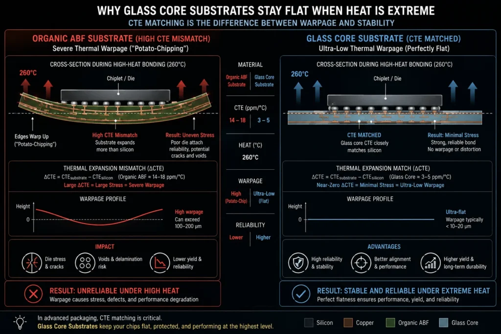
Silicon dies have a very low Coefficient of Thermal Expansion (CTE). Organic substrates (like ABF) have a very high CTE. When bonded together at 250°C and then cooled, the organic plastic shrinks violently while the silicon barely moves. This mathematical mismatch (Δα) induces massive thermomechanical stress, causing the entire package to warp into a “potato chip” shape, snapping the microscopic solder bumps connecting the die to the board.
2. The Core Mechanism: Tunable Silicates
Glass resolves this because its CTE can be chemically tuned (typically between 3 to 7 ppm/°C) to perfectly match the silicon dies sitting on top of it. Because both materials expand and contract at the exact same microscopic rate, the thermomechanical stress drops to near-zero, allowing the package to remain flawlessly flat even at massive scale (>100mm per side).
3. Technical Depth: Through-Glass Vias (TGVs)
To move power and data vertically through the solid glass, engineers must create Through-Glass Vias (TGVs).
Unlike soft plastics, you cannot mechanically drill glass. Instead, the process uses ultrafast picosecond or femtosecond lasers to pulse light through the glass, inducing localized structural damage (laser-induced modification). The glass panel is then submerged in a highly corrosive wet chemical bath (Hydrofluoric acid, HF). The acid aggressively eats away the laser-damaged zones while leaving the pristine glass intact, creating perfectly smooth, vertical holes.
4. Metallization and the Aspect Ratio Limit
Once the holes are etched, they must be filled with copper. This requires Physical Vapor Deposition (PVD) to lay down a titanium/copper seed layer, followed by electroplating to achieve a void-free copper pillar. GCS allows for extreme aspect ratios—vias that are very deep but incredibly narrow (e.g., 15:1 up to 70:1). This allows engineers to pack vias closer together, achieving interconnect densities up to 10 times higher than organic cores.
5. Real-World Consequences: High-Frequency Signal Integrity
In traditional silicon interposers, the silicon itself is semi-conductive, which causes parasitic capacitance that degrades ultra-fast electrical signals. Glass is an exceptional insulator with a low dielectric constant (Dk ≈ 2.8) vs silicon’s 12). This means electrical signals traveling at 112G and 224G speeds do not “leak” into the surrounding material, drastically reducing signal attenuation and crosstalk, and saving immense amounts of power in AI data centers.
Commercial Applications for GCS Packaging
Glass core technology is explicitly designed for the highest echelons of data transmission and processing.
Hyperscale AI Accelerators: The primary use case for GCS is housing next-generation GPU complexes. As companies like Nvidia and AMD design architectures that integrate two massive logic dies surrounded by 12 stacks of High Bandwidth Memory (HBM4), the footprint exceeds the physical limit of organic substrates. Glass panels enable these colossal “System-in-Package” (SiP) structures to be assembled flawlessly without buckling under their own massive thermomechanical weight.
Co-Packaged Optics (CPO): Currently, electrical data leaves an AI chip, travels across a motherboard, and is converted to light (optical data) at the front panel of the server. GCS enables Co-Packaged Optics, where the lasers and photonic optical transceivers are bonded directly onto the glass substrate right next to the silicon brain. Because glass is optically transparent and electrically flawless, the data converts from electricity to light instantly, saving massive amounts of power and virtually eliminating latency.
5G/6G RF and Radar Modules: Radio Frequency (RF) components are notoriously sensitive to signal loss and interference. The ultra-low dielectric loss tangent of glass makes it the ultimate substrate for mounting 6G millimeter-wave antennas and automotive radar modules, ensuring pristine signal clarity without the signal bleeding out into the circuit board.
Economic & Strategic Impact
The transition to GCS represents a brutal, multi-billion-dollar resetting of the Advanced Packaging Supply Chain.
For decades, the substrate market was dominated by Japanese firms (like Ajinomoto) producing organic ABF films, and traditional Outsourced Semiconductor Assembly and Test (OSAT) companies.
The pivot to glass requires entirely different manufacturing equipment—femtosecond lasers, massive glass-handling robots, and panel-level lithography tools.Absolics (a subsidiary of South Korea’s SKC) invested $600 million to build the world’s first mass-production GCS facility in Covington, Georgia, aiming to dominate the early market.Simultaneously, TSMC introduced its CoPoS (Chip-on-Panel-on-Substrate) platform, partnering with flat-panel display makers (like Innolux) who already know how to handle massive sheets of glass. This shift threatens to render billions of dollars of legacy organic-substrate manufacturing equipment obsolete, crowning new winners in the global tech supply chain.
Advantages
- Dimensional Stability:The tunable CTE (3-7 ppm/°C) matches silicon, eradicating thermal warpage and allowing the assembly of hyper-massive AI chips larger than 100mm per side.
- Superior Signal Integrity: A lower dielectric constant (D_k) and extremely low insertion loss enable GCS to handle incredibly dense, high-frequency signals (>100 GHz) with up to 40% speed improvements over organic laminates.
- High-Density Interconnects:Smooth glass surfaces and precision laser-etched TGVs allow for redistribution layers (RDL) with trace widths down to 2 micrometers (2/2 µm line/space), allowing ten times the wiring density of standard organics.
- Panel-Level Economics:Manufactured on massive rectangular panels rather than circular wafers, fundamentally improving material utilization and lowering the theoretical cost per unit.
Limitations
- Extreme Fragility and Handling: Glass is brittle. If a massive 510mm panel sustains a microscopic micro-crack on its edge during robot handling, the entire panel can shatter instantaneously, taking dozens of expensive AI packages with it.
- Metallization Complexity: Plating pure copper into a microscopic, 50-to-1 aspect ratio TGV without leaving air voids or suffering delamination is incredibly difficult. If the copper separates from the smooth glass wall inside the via, the chip’s power delivery fails entirely.
- Metrology and Inspection: Because glass is transparent, traditional automated optical inspection (AOI) tools that use light to check for defects on opaque circuit boards become confused. The industry must invent entirely new inspection tools using advanced interferometry to see “inside” the clear glass.
Common Misconceptions
Misconception: Glass core substrates are completely transparent circuit boards.
Reality: While the foundational core is transparent silica glass, the final product is completely covered. Engineers coat both sides of the glass with multiple layers of polymer dielectrics, copper wiring (Redistribution Layers), and solder masks. The final substrate looks like a standard opaque microchip package; the glass is just the hidden spine inside.
Misconception: GCS is competing against TSMC’s CoWoS.
Reality: GCS is an evolution that enhances and eventually replaces parts of CoWoS. Current CoWoS uses a monolithic silicon interposer placed on top of an organic substrate. GCS can replace the bottom organic substrate, or, because it supports such high wiring density, it can eliminate the need for the expensive silicon interposer altogether.
Misconception: The glass used is just like window glass.
Reality: It is ultra-pure, alkali-free specialty glass (similar to borosilicate or advanced quartz) specifically formulated by companies like Corning and SCHOTT. It is engineered at the molecular level to lack impurities that would disrupt electrical signals.
What Most People Miss
The disruptive synergy between Glass Substrates and Flat-Panel Display Makers.
Most analysts view the semiconductor industry in a vacuum. What they miss is that the companies perfectly positioned to build the next generation of AI packaging are the companies that make television and smartphone screens.
Firms like China’s BOE and Taiwan’s Innolux have spent twenty years perfecting the handling, cleaning, and chemical etching of massive, ultra-thin rectangular glass panels for OLED and LCD displays. As TSMC and Intel move packaging away from 300mm circular wafers to panel-level production, they are directly partnering with these display manufacturers. The AI packaging war is quietly resurrecting the flat-panel display industry, transforming TV screen factories into critical nodes for global semiconductor infrastructure.
Comparison Table
| Feature | Organic Substrate (ABF Laminate) | Silicon Interposer | Glass Core Substrate (GCS) |
| Base Material | Woven glass/epoxy resin | Monolithic Silicon Wafer | High-Purity Alkali-Free Glass |
| Warpage Risk (CTE) | Very High (Mismatched) | Low (Matched to Die) | Very Low (Matched & Tunable) |
| Electrical Insulation | Moderate | Poor (Semi-conductive) | Excellent (Ultra-low loss) |
| Max Package Size | Small/Medium | Hard-capped by Reticle Limit | Massive (>100mm per side) |
| Manufacturing Format | Panel-Level | 300mm Circular Wafer | Massive Rectangular Panel |
| Current Status | Market Standard (Hitting limits) | Bottlenecked but Standard | Scaling to HVM (2025-2027) |
Case Study
Situation: The global semiconductor industry faced a physical impasse. High-end AI accelerators required increasingly large substrates to accommodate multiple compute chiplets and HBM stacks. However, scaling traditional organic (ABF) substrates resulted in severe thermal warping, crashing production yields and bottlenecking global AI supply.
Challenge: Develop a rigid, thermally stable substrate capable of sub-2-micron wiring density that could be manufactured at high volumes without the geometric waste associated with traditional 300mm silicon wafers.
Solution (The Absolics Facility): Absolics, a subsidiary of South Korea’s SKC, bypassed incremental improvements and committed to full-scale Glass Core Substrate production. Backed by a $600 million investment and supported by funding from the U.S. CHIPS Act, they constructed a massive, purpose-built manufacturing facility in Covington, Georgia. The facility was engineered to pioneer panel-level TGV laser drilling and metallization at commercial volumes.
Outcome: Entering pilot and early-volume production stages around 2024-2026, the facility marked the first dedicated bet on GCS outside of Intel’s internal R&D lines.By leveraging specialized laser-induced etching and advanced copper paste/PVD metallization techniques, the operation proved that high-aspect-ratio TGVs could be scaled outside of a traditional silicon foundry.
Lessons Learned: The Absolics deployment proved that the transition to glass was not merely a theoretical materials science project, but a bankable infrastructure shift. It validated that the future of advanced packaging relies on separating the substrate manufacturing from the constraints of circular silicon wafers, permanently opening the market to non-traditional, pure-play glass substrate pioneers.
Future Outlook
Next 12–24 Months
The era of Pilot Validation and Supply Chain Formation. Through late 2026 and 2027, the industry will remain in the intensive qualification phase. Intel, Absolics, and Samsung Electro-Mechanics will finalize the reliability testing of their glass packages against the brutal 1,000-hour thermal cycling standards required for server racks. We will see specialized laser equipment suppliers and wet-chemistry vendors (providing advanced HF etching and TGV copper filling solutions) aggressively merge and partner to establish the first end-to-end, standardized GCS manufacturing lines.
Next 3–5 Years
The scaling of High-Volume Manufacturing (HVM). By 2028–2030, GCS will enter the commercial mainstream. The market, growing at an exponential clip toward $8 billion, will see the first major commercial AI accelerators ship on glass backbones. Fan-Out Panel-Level Packaging (FOPLP) will reach maturity, crashing the unit cost of packaging and relieving the global reliance on TSMC’s 300mm CoWoS wafer-level capacity. Glass will rapidly become the baseline requirement for any chip pushing 1.6T or 3.2T network speeds due to its unbeatable signal integrity.
Next 10 Years
The Co-Packaged Optics Singularity. By the mid-2030s, the concept of copper wiring leaving a server rack will be entirely obsolete. Glass Core Substrates will serve as the literal physical medium for Photonic Integrated Circuits (PICs). Lasers will be deeply embedded inside the glass substrate itself, routing light seamlessly between the silicon logic dies through microscopic, 3D-printed optical waveguides carved directly into the glass core. The substrate will cease to be just an electrical board and will become a hybrid electro-optical superhighway, driving AI compute to the physical limits of light.
Most Likely Scenario
Organic laminates will not disappear overnight; they will remain the cheap standard for everyday consumer electronics and standard CPUs. However, for the apex of computing—artificial intelligence, 6G telecom, and data center switching—Glass Core Substrates are the inescapable future. The thermodynamic and electrical walls of plastic have been hit. The hyperscale tech industry is officially entering the era of glass.
Key Takeaways
- Glass Core Substrates (GCS) replace traditional organic (plastic) circuit boards with high-purity glass, solving the massive heat and warping issues that plague large AI chips.
- Glass has a tunable Coefficient of Thermal Expansion (CTE) that perfectly matches silicon. Because they expand at the exact same rate when heated, the package stays perfectly flat, saving the delicate microscopic connections.
- Data travels vertically through the glass via Through-Glass Vias (TGVs). These holes cannot be drilled mechanically; they are created using ultrafast lasers and acid etching, then filled with copper.
- Glass is an exceptional electrical insulator (low dielectric constant). It prevents ultra-high-speed signals (like 224G networking) from leaking or degrading, delivering massive speed and power efficiencies.
- GCS enables Panel-Level Packaging (FOPLP). Instead of using small, circular silicon wafers, foundries can print chips on massive rectangular glass panels, drastically increasing production output and lowering costs.
- The primary challenge is fragility and handling. If a microscopic crack forms on the edge of a massive glass panel during robot handling, the entire panel can shatter instantly.
Glossary
Coefficient of Thermal Expansion (CTE): A measurement of how much a material expands when heated. A mismatch in CTE between two glued materials causes them to violently warp and bend.
Dielectric Constant (D_k): A measure of a material’s ability to store electrical energy. A lower D_k (like glass) is highly desirable in chip packaging because it means electrical signals can travel faster with less interference.
Fan-Out Panel-Level Packaging (FOPLP): A manufacturing method that packages microchips on massive rectangular panels (like glass or organic sheets) instead of traditional circular silicon wafers, greatly increasing yield and efficiency.
Organic Substrate (ABF): The legacy, green plastic-like material (Ajinomoto Build-up Film) used for the last two decades as the base for almost all computer chips. It warps under extreme heat.
Through-Glass Via (TGV): A microscopic, vertical tunnel created through a glass substrate using lasers and acid, which is then filled with metal (usually copper) to carry electrical signals and power.
Wet Chemical Etching: The use of highly corrosive liquids (like hydrofluoric acid) to dissolve specific parts of a material. Used in GCS to carve out the laser-damaged zones into perfect vertical holes.
Sources
Yole Group: Glass Core substrates: the new race for advanced packaging giants (June 2024)
Yole Group: Glass Core substrates: the new race for advanced packaging giants – Challenges and Investments (June 2024)
Exponential Industry: Glass Core Substrates & Interposers: 2026 AI Packaging Guide (August 2026)
Research and Markets: The Global Market for Glass Substrates for Semiconductors 2026-2036
TheElec: Intel and TSMC Push Panel-Level Packaging as Market Sets to Expand Tenfold (July 2026)
PMC: Application of Through Glass Via (TGV) Technology for Sensors Manufacturing and Packaging
HCVAC: A Comprehensive Guide to Through-Glass Via TGV Manufacturing Process and Core Technologies (July 2026)