Advertisement
)

You can design the most advanced, mathematically perfect artificial intelligence chip in human history, but it is completely useless if it cannot access memory fast enough. As AI models scale into the trillions of parameters, processors must pull massive datasets from memory chips thousands of times a second. Traditional green circuit boards are vastly too slow, and their copper wires are spaced too far apart. To solve this “memory wall,” the semiconductor industry no longer just prints chips; they print microscopic silicon bridges to fuse the chips together.
This bridge is called a silicon interposer. It is a highly engineered foundational slab of silicon that acts as an ultra-dense superhighway, linking a GPU directly to its High Bandwidth Memory (HBM). Why should you care right now? Because manufacturing this bridge is the single greatest chokepoint in the global tech economy. Packaging massive, multi-chip AI super-processors is so incredibly difficult and defect-prone that it has hard-capped the global supply of AI hardware. The battle to control this bottleneck—specifically TSMC’s CoWoS packaging capacity—dictates which trillion-dollar tech giants will dominate the next decade and which will be starved of computing power.
What are Silicon Interposers (CoWoS)?
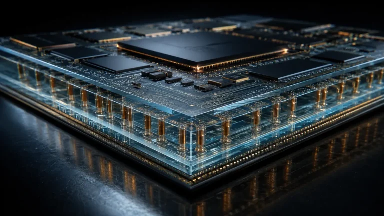
Silicon Interposers in CoWoS (Chip-on-Wafer-on-Substrate) packaging are foundational semiconductor layers used to connect high-performance logic chips with memory components.Featuring microscopic horizontal routing and vertical Through-Silicon Vias (TSVs), the interposer enables ultra-fast, high-density data transmission between chips, bypassing the speed limitations of traditional printed circuit boards.
At a Glance
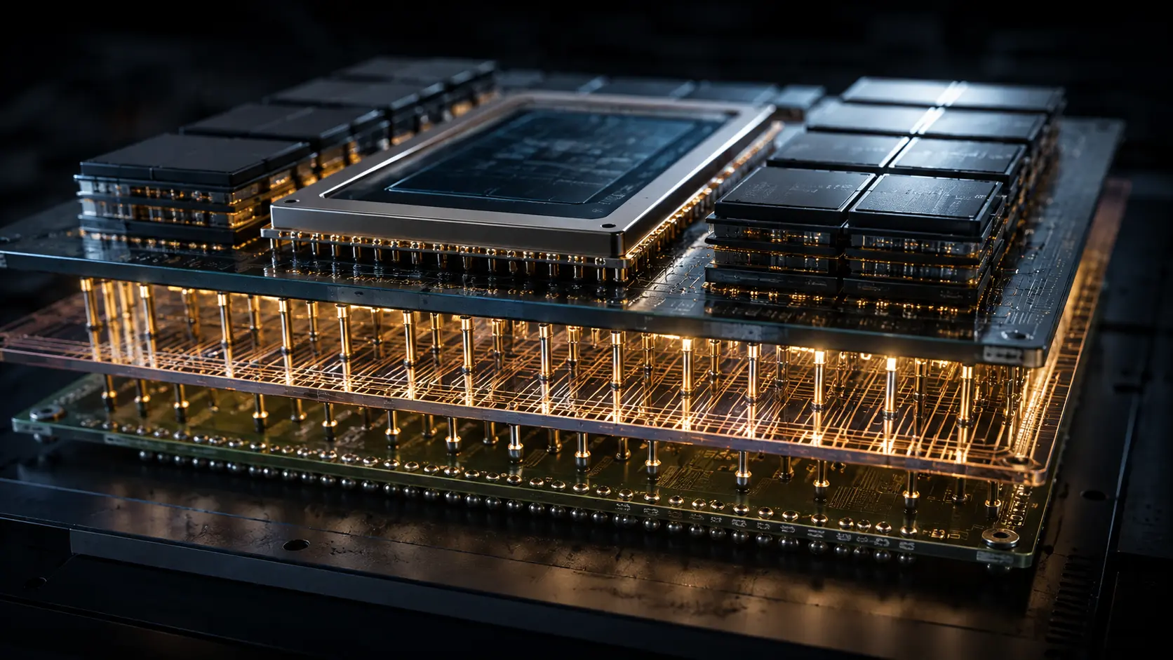
- Concept: Instead of placing two chips on a slow plastic motherboard, engineers place both chips side-by-side onto a third, underlying piece of silicon (the interposer) that contains microscopic, high-speed wiring.
- Why it matters: AI models require extreme bandwidth. The interposer allows tens of thousands of microscopic wires to connect a GPU to HBM, delivering terabytes of data per second.
- Who uses it: Nvidia, AMD, and custom hyperscaler silicon (Google TPU, AWS Trainium) rely almost exclusively on TSMC’s CoWoS packaging.
- Biggest takeaway:As companies design larger AI chips (combining multiple GPUs and 8 to 12 memory stacks), the physical interposer must grow. If the massive silicon bridge warps by even a few micrometers during the heating process, the entire $40,000 AI chip is destroyed.
In Simple Words
Think of a traditional computer motherboard as a sprawling city. The processor is the downtown office, and the memory is the suburban library. To get information, a commuter (data) has to drive on a highway (copper traces on the green circuit board) that is wide, slow, and constantly fighting traffic.
A silicon interposer tears up the highway and builds a microscopic bullet-train network right next door. Instead of placing the processor and the memory on a plastic circuit board, engineers place both of them side-by-side onto a highly engineered slab of silicon (the interposer).
Because the interposer is made of the exact same pure silicon as the chips themselves, the wires connecting them can be printed unimaginably small and dense. The data no longer travels across a city; it steps across a millimeter-wide bridge, arriving instantly.
Why This Matters
For Semiconductor Engineers and Supply Chain Executives, CoWoS packaging capacity is the ultimate metric of AI market dominance.
Global CoWoS demand is projected to double from roughly 1.3 million wafers in 2026 to over 2.5 million by 2027. Nvidia alone has pre-booked over 50% of TSMC’s total CoWoS output through multi-year, multi-billion-dollar prepayment commitments. If a rival chipmaker designs an AI accelerator that beats Nvidia on paper, it is economically irrelevant if they cannot secure the CoWoS interposer capacity to actually package and ship it. Understanding the yield constraints of the silicon interposer is the only way to accurately forecast hardware delivery timelines in the artificial intelligence sector.
The Evolution of Advanced Packaging and Chiplets
The evolution of “Moore’s Law” has fractured. We can no longer shrink transistors fast enough to double performance on a single, monolithic piece of silicon.
To keep performance doubling, the industry pivoted to “Advanced Packaging” (2.5D and 3D integration). Instead of making one giant chip, companies break the processor into smaller “chiplets” and surround them with stacked memory. The silicon interposer is the literal canvas upon which these chiplets are stitched back together. TSMC dominates this space with ~95% of leading-edge capacity because their front-end silicon manufacturing expertise translates perfectly into building flawless, high-density interposers.
How Silicon Interposers and CoWoS Packaging Work
Connecting tens of billions of transistors across separate physical chips without melting the assembly requires extreme materials science. Here is the first-principles breakdown of the CoWoS architecture.
1. The Fundamental Problem: The Organic Pitch Limit
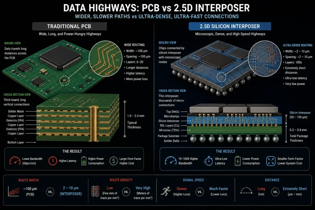
Historically, chips were attached to organic (plastic/resin) substrates using tiny solder balls (C4 bumps). However, organic substrates cannot support wires closer than roughly 15 to 20 micrometers apart without short-circuiting. An AI processor needs tens of thousands of connections to its memory, making the organic pitch limit a fatal data bottleneck.
2. The Insufficiency of Monolithic Silicon
Building the GPU and the HBM memory together on the exact same piece of silicon is impossible. They require entirely different manufacturing nodes and chemical processes. They must be manufactured separately and combined later.
3. The Core Mechanism: The 2.5D Silicon Interposer
TSMC’s CoWoS inserts a “2.5D” layer. A bare silicon wafer is processed using standard lithography to create microscopic Redistribution Layers (RDL). Because it is silicon, the wires can be placed incredibly close together (sub-micron pitch). The known-good GPU dies and HBM stacks are micro-bumped and soldered perfectly side-by-side onto the top of this silicon interposer.
4. Technical Depth: Through-Silicon Vias (TSVs)
The interposer solves horizontal data movement, but power and external data must still flow vertically down into the main motherboard. To accomplish this, engineers use Through-Silicon Vias (TSVs). A deep, microscopic hole is etched via a Bosch process entirely through the silicon interposer and filled with copper.
These TSVs must have extreme aspect ratios (depth vs. width). If the copper is poorly deposited, electromigration occurs, or parasitic capacitance and inductance severely degrade the signal transmission rate.
5. Real-World Consequences: CTE Mismatch and Thermal Warpage
Once the GPU and HBM are attached to the interposer (Chip-on-Wafer), the entire silicon assembly must be attached to the organic substrate below it.
This thermal bonding process is perilous. Silicon expands slowly when heated; organic plastic expands rapidly. This difference in the Coefficient of Thermal Expansion (CTE) causes the massive interposer to violently bow and warp during heating. If the interposer warps beyond a few micrometers, the delicate micro-bumps snap, permanently destroying the assembly and resulting in a total yield loss.
Commercial Applications for CoWoS Interposers
The physical scaling of the silicon interposer directly maps to the performance ceiling of enterprise artificial intelligence.
Hyperscale AI Accelerators (Nvidia Blackwell/Rubin): Nvidia’s architectural leaps are gated by interposer size. Their previous generation utilized a roughly 3.3x reticle limit to fit one GPU and six HBM stacks. The upcoming Vera Rubin architectures demand massive CoWoS-L interposers capable of housing two compute dies and up to 12 HBM4 stacks, driving multi-hundred-thousand wafer annual demand and pushing TSMC to expand limits to 5.5x and eventually 9x.
High-Performance Computing (HPC) CPUs: Beyond pure AI, server CPUs (like AMD’s EPYC and MI series) utilize interposers to fuse disparate chiplets together. By placing a centralized I/O die and multiple compute chiplets on an interposer, AMD can achieve the performance of a massive monolithic chip without suffering the ruinous defect rates of trying to print a single 800 mm² piece of silicon.
Advanced Image Sensors: While not requiring massive interposers, CMOS image sensors were the original proving ground for Through-Silicon Vias (TSVs). By using TSVs to route connections vertically, camera manufacturers eliminated bulky edge-wiring, allowing them to stack the photodiode directly on top of the signal readout layer, drastically reducing the physical footprint of smartphone cameras.
Economic & Strategic Impact
The economics of CoWoS dictate a massive capital expenditure (CapEx) moat that highly shields TSMC from competitors.
A fully processed CoWoS wafer costs an estimated $10,000, achieving gross margins well above TSMC’s corporate average.Because packaging requires front-end-like processes (photolithography, chemical vapor deposition, precise copper plating for TSVs), legacy backend Outsourced Semiconductor Assembly and Test (OSAT) companies like ASE and Amkor struggled to compete immediately.
While OSATs are rapidly acquiring the tools to handle the substrate-attachment phase (oSoS – OSAT on Substrate), TSMC maintains an iron grip on the highly lucrative Chip-on-Wafer (CoW) interposer fabrication phase. This dynamic effectively centralizes the total addressable market of advanced AI packaging revenue into the Taiwanese supply chain.
Advantages
- Ultra-High Interconnect Density: Silicon interposers allow for routing pitches below 1 micrometer, delivering terabytes of memory bandwidth completely unattainable on standard organic PCBs.
- Reduced Power Consumption: The microscopic distance between the GPU and the HBM means data does not have to be blasted across a long copper wire, drastically reducing the energy (picojoules per bit) required for memory retrieval.
- Chiplet Economics: Enables the “System-in-Package” (SiP) era. Companies can manufacture their GPU on an expensive 3nm node, manufacture their I/O on a cheaper 6nm node, and bridge them together flawlessly, optimizing fab costs.
Limitations
- The Reticle Size Ceiling: Photolithography machines can only expose a maximum area of roughly 858 mm² (the reticle limit). Building interposers larger than this requires complex “stitching” of multiple exposures, heavily increasing defect rates.
- Circular Wafer Edge Waste: Interposers are massive squares being cut out of a 300mm circular wafer. Geometry dictates that edge material is heavily wasted, keeping material utilization rates below 70% for large AI packages and inflating unit costs.
- Extreme Warpage and Assembly Risk: The larger the silicon interposer, the more severe the CTE mismatch with the organic substrate. If a massive 5.5x reticle package warps during final assembly, the manufacturer loses tens of thousands of dollars of known-good silicon in a single second.
Common Misconceptions
Misconception: The interposer does computations and makes the chip faster.
Reality: The interposer is completely “passive.” It possesses no transistors, no logic gates, and does zero computation. It is entirely a piece of routing infrastructure—a dummy bridge made of ultra-pure silicon designed purely to let the active chips talk to each other. (Note: CoWoS-L integrates small active Local Silicon Interconnects, but the bulk interposer remains passive)
Misconception: More TSVs automatically make the interposer better.
Reality: TSVs are structural liabilities. Drilling too many holes through the silicon weakens the interposer mechanically and induces severe thermo-mechanical stress on the surrounding layers. Optimizing the TSV pitch to balance electrical bandwidth with mechanical integrity is a highly guarded trade secret.
Misconception: Packaging is the cheap, final step of making a chip.
Reality: In the AI era, the silicon interposer and CoWoS process frequently cost more than half of the total package value. “Advanced packaging” has merged with front-end foundry lithography, shedding its historical status as a low-margin backend service.
What Most People Miss
The strategic pivot to CoWoS-L (Local Silicon Interconnects).
Early AI chips used CoWoS-S, which relied on a single, massive, monolithic slab of silicon for the interposer. As chips grew, these massive slabs became too expensive and prone to cracking.
What most observers miss is TSMC’s shift to CoWoS-L. Instead of a single giant silicon slab, CoWoS-L uses a cheaper organic Redistribution Layer (RDL) as the base, and embeds tiny, high-density silicon bridges (Local Silicon Interconnects – LSI) only exactly where the GPU needs to cross over to the HBM.This hybrid approach slashes the total amount of silicon used, mitigates massive thermal warpage, and allows TSMC to push toward the colossal 9x reticle limits promised for 2027.
Comparison Table
| Feature | Standard Flip-Chip (PCB) | CoWoS-S (Silicon Interposer) | CoWoS-L (Local Silicon Interconnect) |
| Routing Base | Organic Substrate | Monolithic Silicon Wafer | Organic RDL + Silicon Bridges |
| Wiring Density (Pitch) | Low (15µm+) | Extreme (<1µm) | Extreme at bridge (<1µm) |
| Thermal Warpage Risk | Low | Very High | Moderate (Stress buffered) |
| Cost Profile | Very Low | Very High | High |
| Maximum Size Scaling | Virtually Unlimited | Hard Capped by Reticle Limits | Highly Scalable (Up to 9x reticle) |
Case Study
Situation: As generative AI models exponentially increased in parameter count throughout the mid-2020s, hardware manufacturers demanded packaging solutions capable of housing increasingly massive logic dies surrounded by 8 to 12 stacks of next-generation HBM.
Challenge: Expanding the silicon interposer beyond the standard 3.3x reticle limit without succumbing to catastrophic yield loss caused by thermal warpage and TSV defect accumulation.
Solution (The 5.5x Reticle Breakthrough): TSMC successfully transitioned its manufacturing lines to support CoWoS-L packages accommodating a die area equivalent to 5.5 times the reticle limit (roughly 4,720 mm² of silicon). They achieved this by optimizing the hybrid RDL-plus-LSI architecture, which acted as a stress buffer against the CTE mismatch inherent in such a massive footprint.
Outcome: By mid-2026, TSMC established an astonishing 98% baseline yield for these massive 5.5x CoWoS-L packages. This allowed only 1-2% of the ultra-expensive assemblies to fail during final bonding, officially validating the mass-production viability of next-generation accelerators like Nvidia’s Rubin architecture and AMD’s Helios configurations.
Lessons Learned: The milestone proved that the physical limits of Moore’s Law can be bypassed through architectural hybridization. By intelligently substituting monolithic silicon interposers with localized bridges embedded in flexible organic layers, foundries can safely scale total package area, ensuring that memory bandwidth constraints do not throttle the AI revolution.
Future Outlook
Next 12–24 Months
The era of 9x Reticle Scaling and HBM4 Integration. In 2027, TSMC will qualify its “Super Carrier” CoWoS platform, pushing the interposer to a massive 9x reticle size (over 7,700 mm²). This footprint is physically required to surround next-gen logic dies with twelve stacks of HBM4 memory. During this window, power supply and cooling will become the secondary bottlenecks; packages of this size will dissipate several kilowatts of heat, forcing data centers into mandatory direct-to-chip liquid cooling or total immersion cooling architectures.
Next 3–5 Years
The scaling of Panel-Level Packaging (CoPoS). By the end of the decade, the geometric waste of cutting rectangular interposers out of 300mm circular wafers will become economically unviable. The industry will attempt to shift to Chip-on-Panel-on-Substrate (CoPoS), utilizing massive square glass or organic panels (e.g., 510mm x 515mm). If lithography toolmakers (like ASML and Canon) can solve the sub-micron alignment accuracy issues on panel-level machinery, the unit cost of AI packaging will crash, radically decentralizing the supply chain.
Next 10 Years
The 3D SoIC Hybrid Bonding Transition. By the 2030s, the 2.5D interposer bridge will reach its ultimate physical limit. The industry will pivot aggressively to true 3D stacking via System on Integrated Chips (SoIC). Instead of using a bridge and micro-bumps, chips will be stacked vertically on top of one another, utilizing direct copper-to-copper hybrid bonding. TSMC aims to reduce this bonding pitch to 4.5 microns by 2029, achieving 50 times the interconnect density of 2.5D interposers, effectively folding a massive AI supercomputer into a vertically stacked, three-dimensional cube.
Most Likely Scenario
Silicon interposers are the definitive linchpin of the 2020s artificial intelligence boom. While true 3D stacking looms on the horizon, the thermal realities of stacking high-heat GPUs vertically ensure that 2.5D CoWoS packaging will remain the undisputed, high-margin workhorse of the industry. The entity that controls interposer yield and TSV aspect ratios controls the physical speed limit of global AI deployment.
Key Takeaways
- Silicon Interposers are foundational layers used in 2.5D packaging to connect AI processors directly to High Bandwidth Memory (HBM), bypassing slow traditional motherboards.
- TSMC’s CoWoS (Chip-on-Wafer-on-Substrate) dominates this market and is currently the primary supply chain bottleneck preventing faster production of AI chips.
- The interposer utilizes Through-Silicon Vias (TSVs)—microscopic vertical copper pillars—to route electricity and data through the silicon layer down to the main package.
- The primary manufacturing risk is thermal warpage. The massive silicon interposer expands at a different rate than the plastic substrate during heating (CTE mismatch), which can crack the delicate connections and destroy the $40,000 chip.
- As of 2026, TSMC achieved 98% yields on its massive 5.5x reticle CoWoS-L packages, proving that multi-die scaling is commercially stable.
- To build even larger chips, the industry is transitioning to CoWoS-L, which uses tiny silicon bridges embedded in a cheaper organic layer, saving cost and reducing warping risks.
Glossary
2.5D Packaging: A technology where multiple chips are placed side-by-side on a foundational interposer, rather than being stacked vertically (3D) or placed separately on a standard circuit board (2D).
Chip-on-Wafer-on-Substrate (CoWoS): TSMC’s proprietary, industry-leading 2.5D packaging technology that integrates logic dies and memory onto a silicon interposer.
Coefficient of Thermal Expansion (CTE): A metric describing how much a material expands when heated. CTE mismatches between silicon and organic plastics cause catastrophic warping during manufacturing.
High Bandwidth Memory (HBM): Stacked memory chips that provide extreme data transfer rates, acting as the critical companion to AI GPUs on the interposer.
Reticle Limit: The maximum physical area (roughly 858 mm²) that a semiconductor lithography machine can print in a single exposure. Massive AI chips are measured in multiples of this limit (e.g., 5.5x).
Through-Silicon Via (TSV): A vertical electrical connection passing completely through a silicon wafer or die, allowing dense vertical data routing.
Frequently Asked Questions
Why can’t we just make the AI chip bigger instead of using an interposer?
Silicon manufacturing is prone to microscopic defects. If you try to print one massive, 2,000 mm² chip, a single dust particle ruins the entire thing, resulting in near-zero yield. It is economically mandatory to print smaller, perfect “chiplets” and stitch them together on an interposer.
Why does Nvidia rely so heavily on TSMC for this?
Packaging is no longer a simple backend process. CoWoS requires extremely precise front-end lithography (like etching TSVs and printing sub-micron wires). TSMC possesses the most advanced, high-yield front-end equipment and capacity on Earth, creating a near-monopoly on advanced 2.5D integration.
What happens if the interposer cracks during manufacturing?
The entire assembly is ruined. Because the highly expensive GPU and HBM chips are permanently soldered to the interposer before it is attached to the main substrate, a crack in the interposer means throwing away tens of thousands of dollars of perfectly good silicon.
Is the silicon interposer a computer chip?
No. A standard CoWoS-S interposer has no transistors and does zero computing. It is entirely a piece of passive infrastructure—a microscopic highway network designed exclusively to move data between the active chips.
Will interposers get cheaper?
Eventually, yes. The industry is attempting to move from 300mm circular wafers (which waste massive amounts of material at the edges when printing giant square packages) to Panel-Level Packaging (CoPoS). If successful, printing on massive rectangular glass panels will drastically lower the cost per interposer.
Sources
Reddit: TSMC ‘Super Carrier’ CoWoS interposer gets bigger, enabling massive AI chips to reach 9-reticle sizes with 12 HBM4 stacks
Exponential Industry: TSMC CoWoS & SoIC Packaging: The AI Supply Bottleneck Explained
TechPowerUp: TSMC Achieves 98% Yield on CoWoS-L with 5.5x Reticle Size, 14x Comes in 2029
TechPowerUp Forums: TSMC Achieves 98% Yield on CoWoS-L with 5.5x Reticle Size
3D InCites: IFTLE 615: TSMC Evolves CoWoS Technology Promising 9x Reticle Size by 2027
Wikipedia: Through-silicon via
Wikipedia: Through-silicon via – Applications & History
Cadence System Analysis: What Are Through-Silicon Vias?
AnySilicon: Understanding CoWoS Packaging Technology
Ginechip: Silicon Interposer for 2.5D/3D Packaging